- 您現在的位置:買賣IC網 > Datasheet目錄42 > LTC4302IMS-1#TRPBF (Linear Technology)IC BUFFER 2-WIRE BUS 10-MSOP Datasheet資料下載
參數資料
| 型號: | LTC4302IMS-1#TRPBF |
| 廠商: | Linear Technology |
| 文件頁數: | 9/20頁 |
| 文件大小: | 298K |
| 描述: | IC BUFFER 2-WIRE BUS 10-MSOP |
| 標準包裝: | 2,500 |
| 類型: | 熱交換開關 |
| 應用: | 通用型緩沖器/總線擴展器 |
| 內部開關: | 是 |
| 電源電壓: | 2.7 V ~ 5.5 V |
| 工作溫度: | -40°C ~ 85°C |
| 安裝類型: | 表面貼裝 |
| 封裝/外殼: | 10-TFSOP,10-MSOP(0.118",3.00mm 寬) |
| 供應商設備封裝: | 10-MSOP |
| 包裝: | 帶卷 (TR) |
LTC4302-1/LTC4302-2
9
sn430212 430212fs
OPERATIO
broken up into 9-bit segments, one byte followed by one
bit for acknowledging. For example, sending out an ad-
dress consists of 7-bits of device address, 1-bit that
signals whether a read or write operation will be per-
formed and then 1 more bit to allow the slave to acknowl-
edge. There is no theoretical limit to how many total bytes
can be exchanged in a given transmission.
I
2
C and SMBus are very similar specifications, SMBus
having been derived from I
2
C. In general, SMBus is
targeted to low power devices (particularly battery pow-
ered ones) and emphasizes low power consumption while
I
2
C is targeted to higher speed systems where the power
consumption of the bus is not as critical. I
2
C has three
different specifications for three different maximum speeds,
these being standard mode (100kHz max), fast mode
(400kHz max), and Hs mode (3.4MHz max). Standard and
fast mode are not radically different, but Hs mode is very
different from a hardware and software perspective and
requires an initiating command at standard or fast speed
before data can start transferring at Hs speed. SMBus
simply specifies a 100kHz maximum speed.
The START and STOP Conditions
When the bus is not in use, both SCL and SDA must be
high. A bus master signals the beginning of a transmission
with a START condition by transitioning SDA from high to
low while SCL is high. When the master has finished
communicating with the slave, it issues a STOP condition
by transitioning SDA from low to high while SCL is high.
The bus is then free for another transmission.
Acknowledge
The acknowledge signal is used for handshaking between
the master and the slave. An acknowledge (LOW active)
generated by the slave lets the master know that the latest
byte of information was received. The acknowledge re-
lated clock pulse is generated by the master. The transmit-
ter master releases the SDA line (HIGH) during the ac-
knowledge clock pulse. The slave-receiver must pull down
the SDA line during the acknowledge clock pulse so that it
remains stable LOW during the HIGH period of this clock
pulse.
When a slave-receiver doesnt acknowledge the slave
address (for example, its unable to receive because its
performing a real-time function), the data line must be left
HIGH by the slave. The master can then generate a STOP
condition to abort the transfer.
If a slave receiver does acknowledge the slave address but
some time later in the transfer cannot receive any more
data bytes, the master must again abort the transfer. This
is indicated by the slave not generating the acknowledge
on the first byte to follow. The slave leaves the data line
HIGH and the master generates the STOP condition. When
the master is reading data from the slave, the master
acknowledges each byte read except for the last byte read.
The master signals a not acknowledge when no other data
is to be read and carries out the STOP condition.
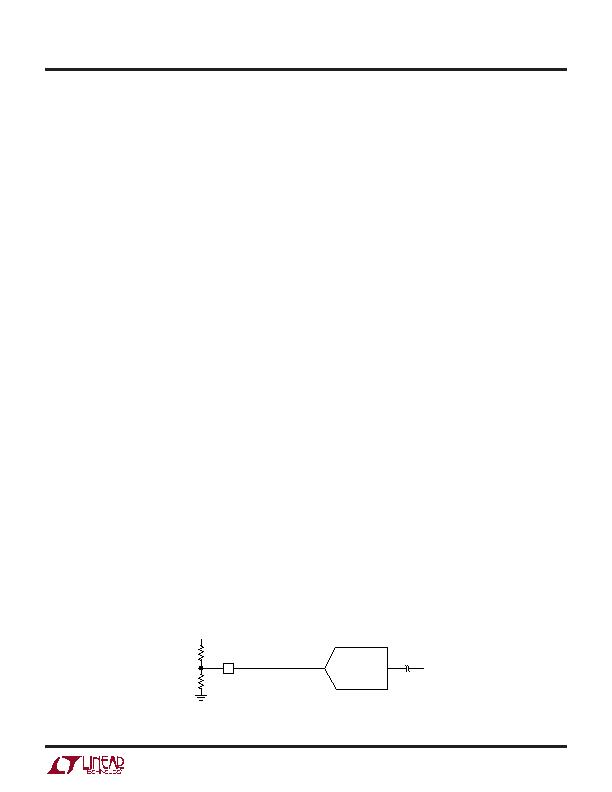
Address Byte and Setting the LTC4302s Address
The LTC4302s address is set by connecting ADDRESS to
a resistive divider between V
CC
and ground. The voltage on
ADDRESS is converted into a 5-bit digital word by an A/D
converter, as shown in Figure 1. This 5-bit word sets the
5 LSBs of the LTC4302s address; its two MSBs are
always
11
. Using 1% resistors, the voltage at ADDRESS
is set 0.5LSB away from each code transition. For ex-
ample, with V
CC
=5V, 1LSB=5V/32 codes = 156.25mV/
code. To set an address of 00, set ADDRESS to 0V +
0.5LSB = 78.125mV.
5-BIT
A/D
4302 F01
ADDRESS
4
5 WIRE
R1
R2
V
CC
Figure 1. Address Compare Circuitry
相關PDF資料 |
PDF描述 |
|---|---|
| LTC4303CDD#TRPBF | IC BUS BUFFER I2C 8-DFN |
| LTC4304IDD#TRPBF | IC BUS BUFFER I2C 10-DFN |
| LTC4307IMS8-1#TRPBF | IC BUFFER 2-WIRE BUS 8-MSOP |
| LTC4307IMS8#TRPBF | IC BUS BUFFER I2C 8-MSOP |
| LTC4308IMS8#TRPBF | IC BUS BUFFER LV 8-MSOP |
相關代理商/技術參數 |
參數描述 |
|---|---|
| LTC4302IMS-2 | 功能描述:IC BUFFER BUS 2WR ADDRESS 10MSOP RoHS:否 類別:集成電路 (IC) >> PMIC - 熱交換 系列:- 產品培訓模塊:Obsolescence Mitigation Program 標準包裝:100 系列:- 類型:熱插拔開關 應用:通用 內部開關:是 電流限制:可調 電源電壓:9 V ~ 13.2 V 工作溫度:-40°C ~ 150°C 安裝類型:表面貼裝 封裝/外殼:10-WFDFN 裸露焊盤 供應商設備封裝:10-TDFN-EP(3x3) 包裝:管件 |
| LTC4302IMS-2#PBF | 功能描述:IC BUFFER 2-WIRE BUS 10-MSOP RoHS:是 類別:集成電路 (IC) >> PMIC - 熱交換 系列:- 產品培訓模塊:Obsolescence Mitigation Program 標準包裝:100 系列:- 類型:熱插拔開關 應用:通用 內部開關:是 電流限制:可調 電源電壓:9 V ~ 13.2 V 工作溫度:-40°C ~ 150°C 安裝類型:表面貼裝 封裝/外殼:10-WFDFN 裸露焊盤 供應商設備封裝:10-TDFN-EP(3x3) 包裝:管件 |
| LTC4302IMS-2#TR | 功能描述:IC BUFFER BUS 2WR ADDRESS 10MSOP RoHS:否 類別:集成電路 (IC) >> PMIC - 熱交換 系列:- 產品培訓模塊:Obsolescence Mitigation Program 標準包裝:100 系列:- 類型:熱插拔開關 應用:通用 內部開關:是 電流限制:可調 電源電壓:9 V ~ 13.2 V 工作溫度:-40°C ~ 150°C 安裝類型:表面貼裝 封裝/外殼:10-WFDFN 裸露焊盤 供應商設備封裝:10-TDFN-EP(3x3) 包裝:管件 |
| LTC4302IMS-2#TRPBF | 功能描述:IC BUFFER 2-WIRE BUS 10-MSOP RoHS:是 類別:集成電路 (IC) >> PMIC - 熱交換 系列:- 產品培訓模塊:Obsolescence Mitigation Program 標準包裝:100 系列:- 類型:熱插拔開關 應用:通用 內部開關:是 電流限制:可調 電源電壓:9 V ~ 13.2 V 工作溫度:-40°C ~ 150°C 安裝類型:表面貼裝 封裝/外殼:10-WFDFN 裸露焊盤 供應商設備封裝:10-TDFN-EP(3x3) 包裝:管件 |
| LTC4303CDD | 制造商:Linear Technology 功能描述:Hot Swappable Bus Buffer 8-Pin DFN EP |
發布緊急采購,3分鐘左右您將得到回復。