- 您現在的位置:買賣IC網 > PDF目錄16707 > MAX14535EEVKIT+ (Maxim Integrated Products)KIT EVAL MAX14535E PDF資料下載
參數資料
| 型號: | MAX14535EEVKIT+ |
| 廠商: | Maxim Integrated Products |
| 文件頁數: | 6/13頁 |
| 文件大小: | 0K |
| 描述: | KIT EVAL MAX14535E |
| 產品培訓模塊: | Lead (SnPb) Finish for COTS Obsolescence Mitigation Program |
| 標準包裝: | 1 |
| 主要目的: | 接口,模擬開關 |
| 嵌入式: | 否 |
| 已用 IC / 零件: | MAX14535E |
| 主要屬性: | 1 x DPDT 開關 |
| 次要屬性: | 2.4 V ~ 5.5 V 電源 |
| 已供物品: | 板 |
MAX14535E–MAX14539E
Low-Resistance DPDT Switches
with Negative Rail
2
_______________________________________________________________________________________
ABSOLUTE MAXIMUM RATINGS
ELECTRICAL CHARACTERISTICS
(VCC = +2.4V to +5.5V, TA = -40°C to +85°C, unless otherwise noted. Typical values are at VCC = +3.0V, TA = +25°C.) (Note 2)
Stresses beyond those listed under “Absolute Maximum Ratings” may cause permanent damage to the device. These are stress ratings only, and functional
operation of the device at these or any other conditions beyond those indicated in the operational sections of the specifications is not implied. Exposure to
absolute maximum rating conditions for extended periods may affect device reliability.
Note 1: Package thermal resistances were obtained using the method described in JEDEC specification JESD51-7 using a four-
layer board. For detailed information on package thermal considerations, refer to www.maxim-ic/thermal-tutorial.
(Voltages referenced to GND.)
VCC, CB, EN ..........................................................-0.3V to +6.0V
NO_, NC_, COM_ (VCC > 2.4V, MAX14535E/
MAX14536E/MAX14539E).................................-1.8V to +3.6V
NO_, NC_, COM_ (VCC < 2.4V, MAX14535E/
MAX14536E/MAX14539E).................................-0.3V to +3.6V
NO_, NC_, COM_ (VEN < VIL, MAX14537E/
MAX14538E)......................................................-0.3V to +6.0V
NO_, NC_, COM_ (VEN > VIL, VCC > 2.4V,
MAX14537E/MAX14538E).................................-1.8V to +3.6V
NO_, NC_, COM_ (VEN < VIL, VCC < 2.4V,
MAX14537E/MAX14538E).................................-0.3V to +3.6V
Continuous Current into NO_, NC_, COM_ Terminals....±300mA
Peak Current into NO_, NC_,
COM_ Terminals (50% duty cycle).............................±500mA
Continuous Power Dissipation (TA = +70°C)
10-Pin UTQFN (derate 6.9mW/°C above +70°C).........559mW
Junction-to-Ambient Thermal Resistance (
θJA) (Note 1)..143.1°C/W
Junction-to-Case Thermal Resistance (
θJC) (Note 1)...20.1°C/W
Operating Temperature Range ...........................-40°C to +85°C
Storage Temperature Range .............................-65°C to +150°C
Junction Temperature Range ............................-40°C to +150°C
Lead Temperature (soldering, 10s) .................................+300°C
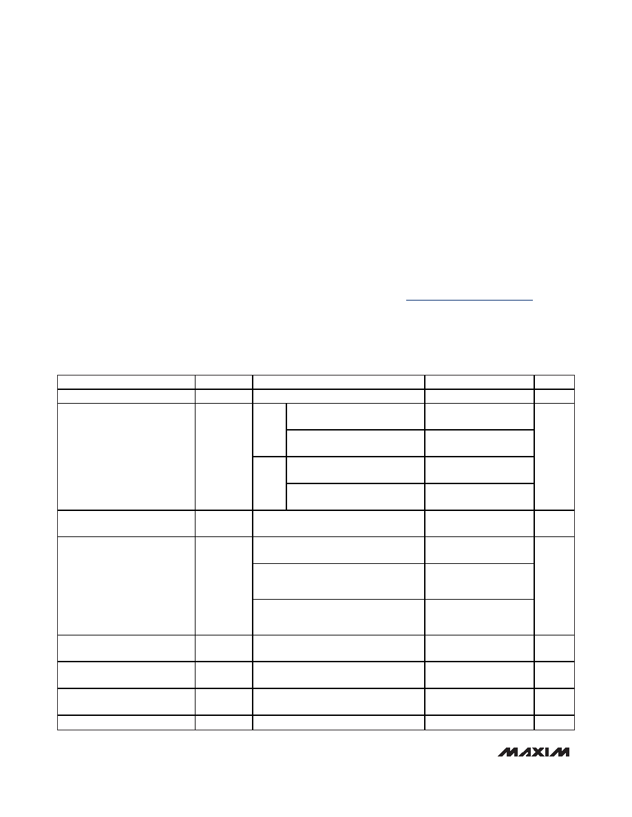
PARAMETER
SYMBOL
CONDITIONS
MIN
TYP
MAX
UNITS
Power-Supply Range
VCC
2.4
5.5
V
MAX14537E/MAX14538E,
VEN = 0
1
VCC =
3.0V
MAX14535E/MAX14536E/
MAX14539E, VEN = 0, VEN = VCC
815
MAX14537E/MAX14538E,
VEN = 0
1
Supply Current
ICC
VCC =
5.5V
MAX14535E/MAX14536E/
MAX14539E, VEN = 0, VEN = VCC
12
25
A
Supply Current Increase with
Logic Level
VEN = 0.4V or 1.4V, VCB = 0.4V or 1.4V
5
A
MAX14537E/MAX14538E,
VEN < VIL
0VCC
MAX14537E/MAX14538E,
VEN > VIH
-1.5
Min
(3.0V,
VCC)
Analog Signal Range
MAX14535E/MAX14536E/MAX14539E
-1.5
Min
(3.0V,
VCC)
V
On-Resistance
RON
VCC = 3.0V, VCOM_ = -1.5V, 3.0V;
INO_ = 100mA or INC_ = 100mA
0.135
0.35
On-Resistance Match Between
Channels
RON
VCC = 3.0V, VCOM_ = 0; ICOM_ = 100mA
(Note 3)
0.05
On-Resistance Flatness
RFLAT(ON)
VCC = 3.0V, ICOM_ = 100mA;
VCOM_ = -1.5V to +3.0V (Note 4)
0.3
1
m
Shunt Switch Resistance
RSH
INO_ or INC_ = 1mA
500
1000
相關PDF資料 |
PDF描述 |
|---|---|
| ZR431C01STZ | IC VREF SHUNT PREC ADJ TO-92-3 |
| EMC13DREH-S13 | CONN EDGECARD 26POS .100 EXTEND |
| V72B5E150B2 | CONVERTER MOD DC/DC 5V 150W |
| SC75-330 | INDUCTOR SMD 33UH 1.20A 2.52MHZ |
| RBA24DTKH | CONN EDGECARD 48POS DIP .125 SLD |
相關代理商/技術參數 |
參數描述 |
|---|---|
| MAX14535EEVKIT+ | 功能描述:交換機 IC 開發工具 MAX14535E Eval Kit RoHS:否 制造商:Maxim Integrated 產品:Evaluation Kits 類型:USB Power Switches 工具用于評估:MAX4984E 工作電源電壓:2.8 V to 5.5 V |
| MAX14536EEVB+ | 功能描述:IC SWITCH DPDT 10UTQFN RoHS:是 類別:集成電路 (IC) >> 接口 - 模擬開關,多路復用器,多路分解器 系列:- 產品培訓模塊:Obsolescence Mitigation Program 標準包裝:2,500 系列:- 功能:- 電路:2 x SPST 導通狀態電阻:20 歐姆 電壓電源:單電源 電壓 - 電源,單路/雙路(±):3 V ~ 5.5 V 電流 - 電源:4.1mA 工作溫度:-40°C ~ 85°C 安裝類型:表面貼裝 封裝/外殼:10-WFDFN 裸露焊盤 供應商設備封裝:10-TDFN-EP(3x3) 包裝:帶卷 (TR) |
| MAX14536EEVB+T | 功能描述:交換機 IC 開發工具 Low-Resistance DPDT Switch w/Neg Rail RoHS:否 制造商:Maxim Integrated 產品:Evaluation Kits 類型:USB Power Switches 工具用于評估:MAX4984E 工作電源電壓:2.8 V to 5.5 V |
| MAX14539EEVB+T | 功能描述:交換機 IC 開發工具 Low-Resistance DPDT Switch w/Neg Rail RoHS:否 制造商:Maxim Integrated 產品:Evaluation Kits 類型:USB Power Switches 工具用于評估:MAX4984E 工作電源電壓:2.8 V to 5.5 V |
| MAX14540AEEWP+T | 制造商:Maxim Integrated Products 功能描述:USB MULTIPLEXER INTERFACE CIRCUITS - Tape and Reel |
發布緊急采購,3分鐘左右您將得到回復。