- 您現(xiàn)在的位置:買賣IC網(wǎng) > PDF目錄16783 > MAX98500EVKIT+ (Maxim Integrated Products)KIT EVAL FOR MAX98500 PDF資料下載
參數(shù)資料
| 型號(hào): | MAX98500EVKIT+ |
| 廠商: | Maxim Integrated Products |
| 文件頁(yè)數(shù): | 5/15頁(yè) |
| 文件大小: | 0K |
| 描述: | KIT EVAL FOR MAX98500 |
| 產(chǎn)品培訓(xùn)模塊: | Lead (SnPb) Finish for COTS Obsolescence Mitigation Program |
| 標(biāo)準(zhǔn)包裝: | 1 |
| 系列: | * |
第1頁(yè)第2頁(yè)第3頁(yè)第4頁(yè)當(dāng)前第5頁(yè)第6頁(yè)第7頁(yè)第8頁(yè)第9頁(yè)第10頁(yè)第11頁(yè)第12頁(yè)第13頁(yè)第14頁(yè)第15頁(yè)
______________________________________________________________________________________ 13
MAX98500
Boosted 2.2W Class D Amplifier
with Automatic Level Control
Supply Bypassing, Layout, and Grounding
Proper layout and grounding are essential for optimum
performance. Use a large continuous ground plane on
a dedicated layer of the PCB to minimize loop areas.
Connect AGND and BSTPGND/SPKPGND directly to the
ground plane using the shortest traces length possible.
Proper grounding improves audio performance, and
prevents any digital noise from coupling into the analog
audio signals.
Bypass VBAT with a 10FF capacitor and a system
bulk capacitance of 22FF or larger. Bypass PVDD to
SPKPGND with a 0.1FF capacitor and with as minimal a
loop area as possible. Connect SPKP and SPKN to the
speaker using the shortest and widest traces possible.
Reducing trace length minimizes radiated EMI. Route
SPKP/SPKN as a differential pair on the PCB to minimize
loop area, thereby, the inductance of the circuit. If filter
components are used on the speaker outputs, be sure
to locate them as close as possible to the MAX98500 to
ensure maximum effectiveness. Minimize the trace length
from any ground-tied passive components to SPKPGND
to further minimize radiated EMI.
An evaluation kit (MAX98500 Evaluation Kit) is available
to provide an example layout for the MAX98500.
WLP Applications Information
For the latest application details on WLP construction,
dimensions, tape carrier information, PCB techniques,
bump-pad layout, and recommended reflow tempera-
ture profile, as well as the latest information on reliability
testing results, refer to the Application Note 1891: Wafer-
Level Packaging (WLP) and Its Applications on Maxim’s
website at www.maxim-ic.com/ucsp. See Figure 4 for the
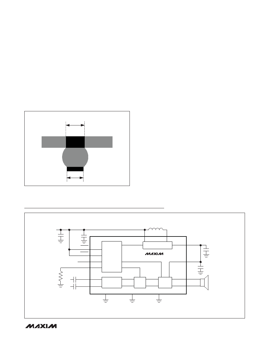
recommended PCB footprint for the MAX98500.
Figure 4. Recommended PCB Footprint
Typical Application Circuit
0.25mm
0.22mm
CONTROL
DIFFERENTIAL
INPUT
BOOST CONVERTER
GAIN
OUTPUT
STAGE
BATTERY
SPKP
SPKN
PVDD
8I
VCCOUT
LX
VBAT
22F*
27.4kI
1%
CIN
1F
CIN
1F
*SYSTEM LEVEL REQUIREMENT
AGND
SPKPGND
BSTPGND
C4
A4
D1, C2
D3
RKNEE B3
GAIN B2
SDSPK C3
SDBST D4
B4
A3
A2
A1
B1
C1
CVBAT
10F
0805
10%
2.2H
20%
INP D2
INN
MAX98500
CVCCOUT
22F
0805
10%
0.1F
10%
相關(guān)PDF資料 |
PDF描述 |
|---|---|
| M1DXA-2636J | IDC CABLE - MKR26A/MC26G/X |
| ESM12DTBH | CONN EDGECARD 24POS R/A .156 SLD |
| RCC10DRTS-S93 | CONN EDGECARD 20POS DIP .100 SLD |
| EGM12DTBH | CONN EDGECARD 24POS R/A .156 SLD |
| OM13005,598 | BOARD EVAL EM773 METER US PLUG |
相關(guān)代理商/技術(shù)參數(shù) |
參數(shù)描述 |
|---|---|
| MAX98500EVKIT+ | 功能描述:音頻 IC 開(kāi)發(fā)工具 MAX98500 Eval Kit RoHS:否 制造商:Texas Instruments 產(chǎn)品:Evaluation Kits 類型:Audio Amplifiers 工具用于評(píng)估:TAS5614L 工作電源電壓:12 V to 38 V |
| MAX98500EWE+ | 制造商:Maxim Integrated Products 功能描述:BOOSTED CLASS D AMPLIFIER WITH ALC - Rail/Tube |
| MAX98500EWE+T | 功能描述:音頻放大器 2.2W Mono Class D Amplifier RoHS:否 制造商:STMicroelectronics 產(chǎn)品:General Purpose Audio Amplifiers 輸出類型:Digital 輸出功率: THD + 噪聲: 工作電源電壓:3.3 V 電源電流: 最大功率耗散: 最大工作溫度: 安裝風(fēng)格:SMD/SMT 封裝 / 箱體:TQFP-64 封裝:Reel |
| MAX98502EVKIT# | 功能描述:放大器 IC 開(kāi)發(fā)工具 MAX98502 Eval Kit RoHS:否 制造商:International Rectifier 產(chǎn)品:Demonstration Boards 類型:Power Amplifiers 工具用于評(píng)估:IR4302 工作電源電壓:13 V to 23 V |
| MAX98502EWE+ | 功能描述:音頻放大器 Boosted Class D Amplifier RoHS:否 制造商:STMicroelectronics 產(chǎn)品:General Purpose Audio Amplifiers 輸出類型:Digital 輸出功率: THD + 噪聲: 工作電源電壓:3.3 V 電源電流: 最大功率耗散: 最大工作溫度: 安裝風(fēng)格:SMD/SMT 封裝 / 箱體:TQFP-64 封裝:Reel |
發(fā)布緊急采購(gòu),3分鐘左右您將得到回復(fù)。