- 您現(xiàn)在的位置:買賣IC網 > PDF目錄385563 > MC100LVEP34DTG (ON SEMICONDUCTOR) 2.5V / 3.3V ECL ±2, ±4, ±8 Clock Generation Chip PDF資料下載
參數(shù)資料
| 型號: | MC100LVEP34DTG |
| 廠商: | ON SEMICONDUCTOR |
| 元件分類: | 時鐘及定時 |
| 英文描述: | 2.5V / 3.3V ECL ±2, ±4, ±8 Clock Generation Chip |
| 中文描述: | 100LVE SERIES, LOW SKEW CLOCK DRIVER, 3 TRUE OUTPUT(S), 0 INVERTED OUTPUT(S), PDSO16 |
| 封裝: | LEAD FREE, TSSOP-16 |
| 文件頁數(shù): | 1/12頁 |
| 文件大小: | 157K |
| 代理商: | MC100LVEP34DTG |
Semiconductor Components Industries, LLC, 2006
November, 2006
Rev. 9
1
Publication Order Number:
MC100LVEP34/D
MC100LVEP34
2.5V / 3.3VECL
÷
2,
÷
4,
÷
8
Clock Generation Chip
The MC100LVEP34 is a low skew
÷
2,
÷
4,
÷
8 clock generation chip
designed explicitly for low skew clock generation applications. The
internal dividers are synchronous to each other, therefore, the common
output edges are all precisely aligned. The V
BB
pin, an internally
generated voltage supply, is available to this device only. For
single
ended input conditions, the unused differential input is
connected to V
BB
as a switching reference voltage. V
BB
may also
rebias AC coupled inputs. When used, decouple V
BB
and V
CC
via a
0.01 F capacitor and limit current sourcing or sinking to 0.5 mA.
When not used, V
BB
should be left open.
The common enable (EN) is synchronous so that the internal
dividers will only be enabled/disabled when the internal clock is
already in the LOW state. This avoids any chance of generating a runt
clock pulse on the internal clock when the device is enabled/disabled
as can happen with an asynchronous control. An internal runt pulse
could lead to losing synchronization between the internal divider
stages. The internal enable flip
flop is clocked on the falling edge of
the input clock; therefore, all associated specification limits are
referenced to the negative edge of the clock input.
Upon start
up, the internal flip
flops will attain a random state; the
master reset (MR) input allows for the synchronization of the internal
dividers, as well as multiple LVEP34s in a system. Single
ended CLK
input operation is limited to a V
CC
≥
3.0 V in PECL mode, or V
EE
≤
3.0 V in NECL mode.
Features
35 ps Output
to
Output Skew
Synchronous Enable/Disable
Master Reset for Synchronization
The 100 Series Contains Temperature Compensation.
PECL Mode Operating Range: V
CC
= 2.375 V to 3.8 V
with V
EE
= 0 V
NECL Mode Operating Range: V
CC
= 0 V
with V
EE
=
2.375 V to
3.8 V
Open Input Default State
LVDS Input Compatible
Pb
Free Packages are Available
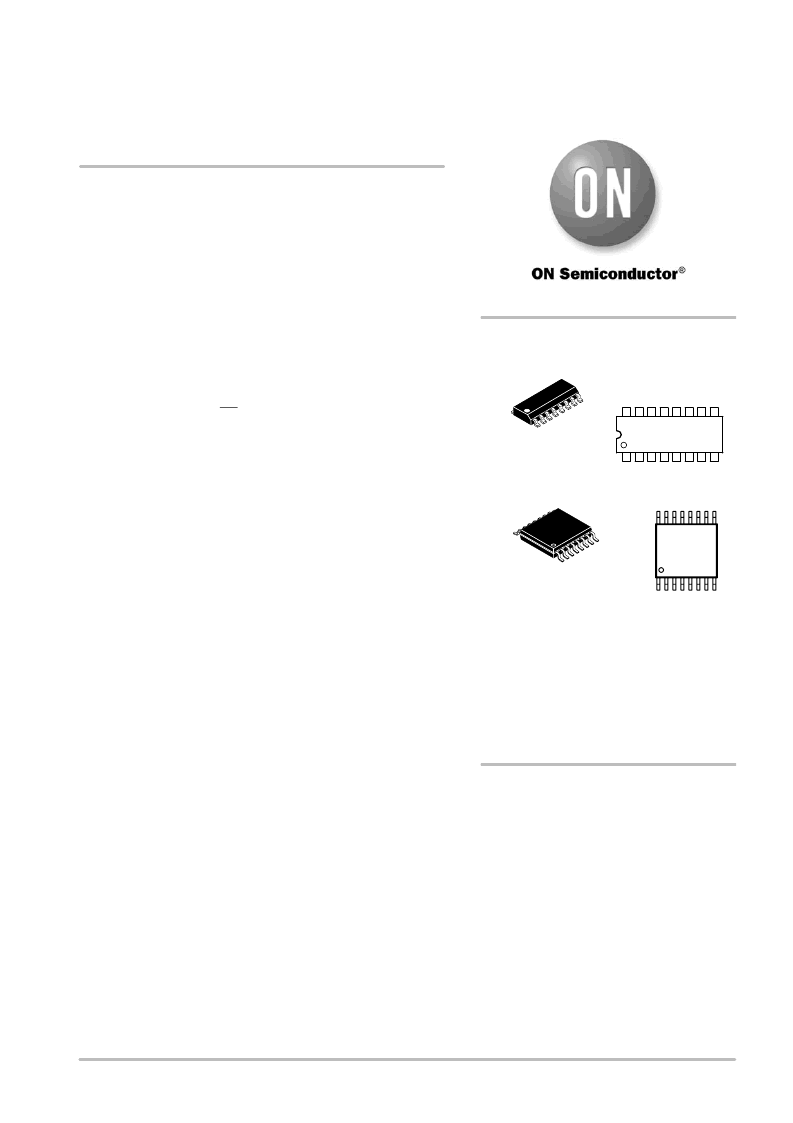
SO
16
D SUFFIX
CASE 751B
1
16
MARKING
DIAGRAMS*
A
L, WL
Y
W, WW = Work Week
G or
= Pb
Free Package
= Assembly Location
= Wafer Lot
= Year
1
16
100LVEP34G
AWLYWW
TSSOP
16
DT SUFFIX
CASE 948F
*For additional marking information, refer to
Application Note AND8002/D.
http://onsemi.com
1
16
100
VP34
ALYW
1
16
See detailed ordering and shipping information in the package
dimensions section on page 8 of this data sheet.
ORDERING INFORMATION
(Note: Microdot may be in either location)
相關PDF資料 |
PDF描述 |
|---|---|
| MC100LVEP34D | 2.5V / 3.3V ECL /2, /4, /8 Clock Generation Chip |
| MC100LVEP34DR2 | 2.5V / 3.3V ECL /2, /4, /8 Clock Generation Chip |
| MC100LVEP34DT | 2.5V / 3.3V ECL /2, /4, /8 Clock Generation Chip |
| MC100LVEP34DTR2 | 2.5V / 3.3V ECL /2, /4, /8 Clock Generation Chip |
| MC100LVEP34DTR2G | 2.5V / 3.3V ECL /2, /4, /8 Clock Generation Chip |
相關代理商/技術參數(shù) |
參數(shù)描述 |
|---|---|
| MC100LVEP34DTG | 制造商:ON Semiconductor 功能描述:LOGIC IC |
| MC100LVEP34DTR2 | 功能描述:時鐘發(fā)生器及支持產品 2.5V/3.3V ECL Clock RoHS:否 制造商:Silicon Labs 類型:Clock Generators 最大輸入頻率:14.318 MHz 最大輸出頻率:166 MHz 輸出端數(shù)量:16 占空比 - 最大:55 % 工作電源電壓:3.3 V 工作電源電流:1 mA 最大工作溫度:+ 85 C 安裝風格:SMD/SMT 封裝 / 箱體:QFN-56 |
| MC100LVEP34DTR2G | 功能描述:時鐘發(fā)生器及支持產品 2.5V/3.3V ECL Clock Generator RoHS:否 制造商:Silicon Labs 類型:Clock Generators 最大輸入頻率:14.318 MHz 最大輸出頻率:166 MHz 輸出端數(shù)量:16 占空比 - 最大:55 % 工作電源電壓:3.3 V 工作電源電流:1 mA 最大工作溫度:+ 85 C 安裝風格:SMD/SMT 封裝 / 箱體:QFN-56 |
| MC100LVGP19DT | 制造商:ON Semiconductor 功能描述: |
| MC100M | 制造商:Thomas & Betts 功能描述:M SERIES BLIND INSERT,MALE |
發(fā)布緊急采購,3分鐘左右您將得到回復。