- 您現在的位置:買賣IC網 > PDF目錄25620 > MC14021BFR1 (ON SEMICONDUCTOR) 4000/14000/40000 SERIES, 8-BIT RIGHT PARALLEL IN SERIAL OUT SHIFT REGISTER, TRUE OUTPUT, PDSO16 PDF資料下載
參數資料
| 型號: | MC14021BFR1 |
| 廠商: | ON SEMICONDUCTOR |
| 元件分類: | 計數移位寄存器 |
| 英文描述: | 4000/14000/40000 SERIES, 8-BIT RIGHT PARALLEL IN SERIAL OUT SHIFT REGISTER, TRUE OUTPUT, PDSO16 |
| 封裝: | EIAJ, PLASTIC, SO-16 |
| 文件頁數: | 1/8頁 |
| 文件大小: | 110K |
| 代理商: | MC14021BFR1 |
Semiconductor Components Industries, LLC, 2005
August, 2005 Rev. 6
1
Publication Order Number:
MC14014B/D
MC14014B, MC14021B
8Bit Static Shift Register
The MC14014B and MC14021B 8bit static shift registers are
constructed with MOS Pchannel and Nchannel enhancement mode
devices in a single monolithic structure. These shift registers find primary
use in paralleltoserial data conversion, synchronous and asynchronous
parallel input, serial output data queueing; and other general purpose
register applications requiring low power and/or high noise immunity.
Features
Synchronous Parallel Input/Serial Output (MC14014B)
Asynchronous Parallel Input/Serial Output (MC14021B)
Synchronous Serial Input/Serial Output
Full Static Operation
“Q” Outputs from Sixth, Seventh, and Eighth Stages
Double Diode Input Protection
Supply Voltage Range = 3.0 Vdc to 18 Vdc
Capable of Driving Two Lowpower TTL Loads or One Lowpower
Schottky TTL Load Over the Rated Temperature Range
MC14014B PinforPin Replacement for CD4014B
MC14021B PinforPin Replacement for CD4021B
PbFree Packages are Available*
MAXIMUM RATINGS (Voltages Referenced to VSS)
Symbol
Parameter
Value
Unit
VDD
DC Supply Voltage Range
0.5 to +18.0
V
Vin, Vout
Input or Output Voltage Range
(DC or Transient)
0.5 to VDD + 0.5
V
Iin, Iout
Input or Output Current
(DC or Transient) per Pin
±10
mA
PD
Power Dissipation, per Package
(Note 1)
500
mW
TA
Ambient Temperature Range
55 to +125
°C
Tstg
Storage Temperature Range
65 to +150
°C
TL
Lead Temperature
(8Second Soldering)
260
°C
Maximum ratings are those values beyond which device damage can occur.
Maximum ratings applied to the device are individual stress limit values (not
normal operating conditions) and are not valid simultaneously. If these limits are
exceeded, device functional operation is not implied, damage may occur and
reliability may be affected.
1. Temperature Derating:
Plastic “P and D/DW” Packages: – 7.0 mW/
_C From 65_C To 125_C
This device contains protection circuitry to guard against damage due to high
static voltages or electric fields. However, precautions must be taken to avoid
applications of any voltage higher than maximum rated voltages to this
highimpedance circuit. For proper operation, Vin and Vout should be constrained
to the range VSS v (Vin or Vout) v VDD.
Unused inputs must always be tied to an appropriate logic voltage level
(e.g., either VSS or VDD). Unused outputs must be left open.
*For additional information on our PbFree strategy and soldering details, please
download the ON Semiconductor Soldering and Mounting Techniques
Reference Manual, SOLDERRM/D.
http://onsemi.com
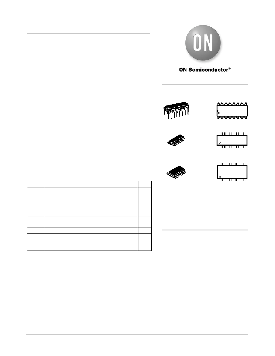
MARKING
DIAGRAMS
PDIP16
P SUFFIX
CASE 648
MC140xxBCP
AWLYYWWG
SOIC16
D SUFFIX
CASE 751B
140xxBG
AWLYWW
xx
= Specific Device Code
A
= Assembly Location
WL, L
= Wafer Lot
YY, Y
= Year
WW, W
= Work Week
G
= PbFree Indicator
SOEIAJ16
F SUFFIX
CASE 966
MC140xxB
ALYWG
See detailed ordering and shipping information in the package
dimensions section on page 6 of this data sheet.
ORDERING INFORMATION
16
1
16
1
16
相關PDF資料 |
PDF描述 |
|---|---|
| MC14027BFL1 | 4000/14000/40000 SERIES, DUAL POSITIVE EDGE TRIGGERED J-K FLIP-FLOP, COMPLEMENTARY OUTPUT, PDSO16 |
| MC14029BCL | 4000/14000/40000 SERIES, SYN POSITIVE EDGE TRIGGERED 4-BIT BIDIRECTIONAL BINARY COUNTER, CDIP16 |
| MC14050BDR2 | 4000/14000/40000 SERIES, HEX 1-INPUT NON-INVERT GATE, PDSO16 |
| MC14175BCLD | 4000/14000/40000 SERIES, POSITIVE EDGE TRIGGERED D FLIP-FLOP, COMPLEMENTARY OUTPUT, CDIP16 |
| MC14512BFEL | 4000/14000/40000 SERIES, 8 LINE TO 1 LINE MULTIPLEXER, TRUE OUTPUT, PDSO16 |
相關代理商/技術參數 |
參數描述 |
|---|---|
| MC14022 | 制造商:ONSEMI 制造商全稱:ON Semiconductor 功能描述:Octal Counter |
| MC14022B | 制造商:Motorola Inc 功能描述: |
| MC14022B_05 | 制造商:ONSEMI 制造商全稱:ON Semiconductor 功能描述:Octal Counter |
| MC14022BCP | 功能描述:計數器移位寄存器 3-18V Octal 4-Stage RoHS:否 制造商:Texas Instruments 計數器類型: 計數順序:Serial to Serial/Parallel 電路數量:1 封裝 / 箱體:SOIC-20 Wide 邏輯系列: 邏輯類型: 輸入線路數量:1 輸出類型:Open Drain 傳播延遲時間:650 ns 最大工作溫度:+ 125 C 最小工作溫度:- 40 C 封裝:Reel |
| MC14022BCPG | 功能描述:計數器移位寄存器 3-18V Octal 4-Stage RoHS:否 制造商:Texas Instruments 計數器類型: 計數順序:Serial to Serial/Parallel 電路數量:1 封裝 / 箱體:SOIC-20 Wide 邏輯系列: 邏輯類型: 輸入線路數量:1 輸出類型:Open Drain 傳播延遲時間:650 ns 最大工作溫度:+ 125 C 最小工作溫度:- 40 C 封裝:Reel |
發布緊急采購,3分鐘左右您將得到回復。