- 您現在的位置:買賣IC網 > PDF目錄382298 > MC145193F (MOTOROLA INC) 1.1 GHZ PLL FREQUENCY SYNTHESIZER PDF資料下載
參數資料
| 型號: | MC145193F |
| 廠商: | MOTOROLA INC |
| 元件分類: | XO, clock |
| 英文描述: | 1.1 GHZ PLL FREQUENCY SYNTHESIZER |
| 中文描述: | PLL FREQUENCY SYNTHESIZER, 1100 MHz, PDSO20 |
| 封裝: | PLASTIC, SO-20 |
| 文件頁數: | 7/24頁 |
| 文件大小: | 240K |
| 代理商: | MC145193F |
MC145193
7
MOTOROLA WIRELESS SEMICONDUCTOR
SOLUTIONS – RF AND IF DEVICE DATA
LOOP SPECIFICATIONS
(VDD = VCC = 2.7 to 5.5 V unless otherwise indicated, TA = –40 to 85
°
C)
Fig.
No.
Guaranteed
Operating
Range
Parameter
Test Condition
Symbol
Min
Max
Unit
Input Sensitivity Range, fin
Input Frequency, REFin Externally Driven in
Reference Mode
100 MHz
≤
fin
≤
1100 MHz
Vin
≥
400 mVpp
7
Pin
fref
– 10
4
dBm*
2.7
≤
VDD < 4.5 V
4.5
≤
VDD
≤
5.5 V
8
1.5
1.5
20
30
MHz
Crystal Frequency, Crystal Mode
C1
≤
30 pF, C2
≤
30 pF, Includes Stray
Capacitance
9
fXTAL
2
15
MHz
Output Frequency, REFout
Operating Frequency of the Phase Detectors
CL = 20 pF, Vout
≥
1 Vpp
10, 12
fout
f
φ
tw
dc
10
MHz
dc
2
MHz
Output Pulse Width (
φ
R,
φ
V, and LD)
fR in Phase with fV, CL = 20 pF,
φ
R and
φ
V
active for LD measurement, **
VPD = 2.7 to 5.5 V
VDD = 2.7 V
VDD = 4.5 V
VDD = 5.5 V
11, 12
40
18
14
120
60
50
ns
Output Transition Times (LD,
φ
V, and
φ
R)
CL = 20 pF, VPD = 2.7 V,
VDD = VCC = 2.7 V
11, 12
tTLH,
tTHL
—
80
ns
Input Capacitance, REFin
*Power level at the input to the dc block.
**When PDout is active, LD minimum pulse width is approximately 5 ns.
Cin
—
7
pF
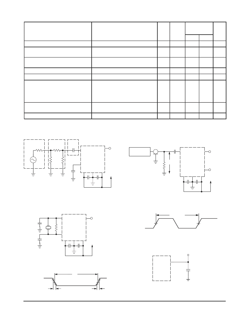
Figure 7. Test Circuit
Sine Wave
Generator
50
Device
Under
Test
0.01
μ
F
Test
Point
VCC
VDD
REFin
Gnd
Output A
Vin
Figure 8. Test Circuit — Reference Mode
(fR)
Test
Point
REFout
V+
Device Under
Test
C1
Test
Point
VCC
VDD
Output A
Gnd
REFin
REFout
C2
Figure 9. Test Circuit — Crystal Mode
(fR)
V+
50%
REFout
1/f REFout
Figure 10. Switching Waveform
10%
90%
Output
tTLH
tTHL
Figure 11. Switching Waveform
50%
tw
Figure 12. Test Circuit
DC
Block
50
PAD
Sine Wave
Generator
50
VCC
VDD
Gnd
V+
Test
Point
Output A
(fV)
Device
Under
Test
fin
fin
NOTE: Alternately, the 50
pad may be a T network.
Test Point
Device
Under
Test
CL*
* Includes all probe and fixture capacitance.
相關PDF資料 |
PDF描述 |
|---|---|
| MC14521B | 24-Stage Frequency Divider |
| MC14521 | 24-Stage Frequency Divider |
| MC14521BCP | Non-inverting High-Speed MOSFET Driver 5-SOT-23 -40 to 125 |
| MC14521BD | 24-Stage Frequency Divider |
| MC14521BDR2 | 24-Stage Frequency Divider |
相關代理商/技術參數 |
參數描述 |
|---|---|
| MC14519BCL | 制造商:Motorola Inc 功能描述: 制造商:Motorola Inc 功能描述:LOGIC MUX, QUAD, 2-INPUT, CMOS, 16 Pin, Ceramic, DIP |
| MC14519BD | 制造商:Rochester Electronics LLC 功能描述:- Bulk |
| MC14519BF | 制造商:Panasonic Industrial Company 功能描述:IC |
| MC1451CCP | 制造商:PMD 功能描述: |
| MC14520B | 制造商:Motorola Inc 功能描述: 制造商:ON Semiconductor 功能描述: |
發布緊急采購,3分鐘左右您將得到回復。