- 您現(xiàn)在的位置:買賣IC網(wǎng) > PDF目錄371031 > MC34065DW-H (MOTOROLA INC) HIGH PERFORMANCE DUAL CHANNEL CURRENT MODE CONTROLLERS PDF資料下載
參數(shù)資料
| 型號(hào): | MC34065DW-H |
| 廠商: | MOTOROLA INC |
| 元件分類: | 穩(wěn)壓器 |
| 英文描述: | HIGH PERFORMANCE DUAL CHANNEL CURRENT MODE CONTROLLERS |
| 中文描述: | 0.4 A DUAL SWITCHING CONTROLLER, 500 kHz SWITCHING FREQ-MAX, PDSO16 |
| 封裝: | PLASTIC, SOP-16 |
| 文件頁數(shù): | 7/16頁 |
| 文件大小: | 419K |
| 代理商: | MC34065DW-H |
MC34065–H, L MC33065–H, L
7
MOTOROLA ANALOG IC DEVICE DATA
Undervoltage Lockout
Two Undervoltage Lockout comparators have been
incorporated to guarantee that the IC is fully functional before
the output stages are enabled. The positive power supply
terminal (VCC) and the reference output (Vref) are each
monitored by separate comparators. Each has built–in
hysteresis to prevent erratic output behavior as their
respective thresholds are crossed. The VCC comparator
upper and lower thresholds are 14 V/10 V for –H suffix, and
8.4 V/7.6 V for –L suffix. The Vref comparator upper and lower
thresholds are 3.6 V/3.4 V respectively. The large hysteresis
and low startup current of the –H suffix version makes it
ideally suited in off–line converter applications where efficient
bootstrap startup techniques are required (Figure 28). The –L
suffix version is intended for lower voltage dc–to–dc
converter applications. The minimum operating voltage for
the –H suffix is 11 V and 8.2 V for the –L suffix.
Drive Outputs and Drive Ground
Each section contains a single totem–pole output stage
that is specifically designed for direct drive of power
MOSFETs. The Drive Outputs are capable of up to
±
400 mA
peak current with a typical rise and fall time of 50 ns with a
1.0 nF load. Additional internal circuitry has been added to
keep the outputs in a sinking mode whenever an
Undervoltage Lockout is active. This characteristic eliminates
the need for an external pull–down resistor. The totem–pole
output has been optimized to minimize cross–conduction
current in high speed operation. The addition of two 10
resistors, one in series with the source output transistor and
one in series with the sink output transistor, reduces the
cross–conduction current to minimal levels, as shown in
Figure 13.
Although the Drive Outputs were optimized for MOSFETs,
they can easily supply the negative base current required by
bipolar NPN transistors for enhanced turn–off (Figure 25).
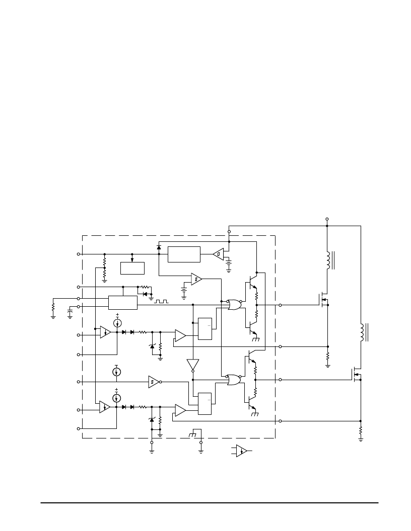
Figure 15. Representative Block Diagram
+
–
–
+
–
+
+
–
+
–
–
+
–
+
12
13
14
5
4
2
3
1
15
7
6
10
11
Vref
Sync Input
RT
CT
Voltage Feedback 1
Compensation 1
Enable Input
Voltage Feedback 2
Compensation 2
Vin= 15V
VCC
16
Q2
RS
Current Sense 2
Drive Output 2
Current Sense 1
Drive Output 1
RS
Q1
10
10
10
10
Gnd
8
Drive Gnd
9
=
Sink Only
Positive True Logic
1.0V
R
S
Q
R
R
PWM
Latch 2
S
R
Q
Current Sense
Comparator 2
2R
Error
Amp 2
Error
Amp 1
Vref
250
μ
A
1.0mA
1.0V
R
1.0mA
Oscillator
3.6V
+
–
20k
Internal
Bias
Reference
Regulator
R
R
2.5V
PWM
Latch 1
VCC
+
–
Current Sense
Comparator 1
Vref
2R
相關(guān)PDF資料 |
PDF描述 |
|---|---|
| MC34065DW-L | HIGH PERFORMANCE DUAL CHANNEL CURRENT MODE CONTROLLERS |
| MC34065DW | Ultra-Small 3-Pin Supply Voltage Supervisor 5-SC70 -40 to 85 |
| MC34065P | Enhanced Product Single Voltage Detector 5-SC70 -55 to 125 |
| MC34065P-H | Enhanced Product Single Voltage Detector 5-SC70 -40 to 125 |
| MC34066DW | HIGH PERFORMANCE RESONANT MODE CONTROLLERS |
相關(guān)代理商/技術(shù)參數(shù) |
參數(shù)描述 |
|---|---|
| MC34065DW-L | 制造商:MOTOROLA 制造商全稱:Motorola, Inc 功能描述:HIGH PERFORMANCE DUAL CHANNEL CURRENT MODE CONTROLLERS |
| MC34065-H | 制造商:ONSEMI 制造商全稱:ON Semiconductor 功能描述:HIGH PERFORMANCE DUAL CHANNEL CURRENT MODE CONTROLLERS |
| MC34065-H_06 | 制造商:ONSEMI 制造商全稱:ON Semiconductor 功能描述:High Performance Dual Channel Current Mode Controllers |
| MC34065-L | 制造商:ONSEMI 制造商全稱:ON Semiconductor 功能描述:High Performance Dual Channel Current Mode Controllers |
| MC34065P | 制造商:MOTOROLA 制造商全稱:Motorola, Inc 功能描述:HIGH PERFORMANCE DUAL CHANNEL CURRENT MODE CONTROLLER |
發(fā)布緊急采購,3分鐘左右您將得到回復(fù)。