- 您現在的位置:買賣IC網 > PDF目錄371031 > MC34065DW-L (MOTOROLA INC) HIGH PERFORMANCE DUAL CHANNEL CURRENT MODE CONTROLLERS PDF資料下載
參數資料
| 型號: | MC34065DW-L |
| 廠商: | MOTOROLA INC |
| 元件分類: | 穩壓器 |
| 英文描述: | HIGH PERFORMANCE DUAL CHANNEL CURRENT MODE CONTROLLERS |
| 中文描述: | 0.4 A DUAL SWITCHING CONTROLLER, 500 kHz SWITCHING FREQ-MAX, PDSO16 |
| 封裝: | PLASTIC, SOP-16 |
| 文件頁數: | 9/16頁 |
| 文件大小: | 419K |
| 代理商: | MC34065DW-L |
MC34065–H, L MC33065–H, L
9
MOTOROLA ANALOG IC DEVICE DATA
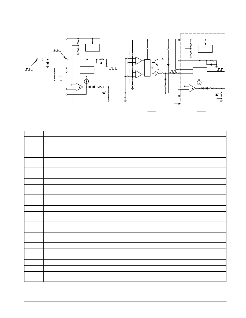
Figure 17. External Clock Synchronization
Figure 18. External Duty Cycle Clamp and
Multi–Unit Synchronization
–
+
R
220pF
RT
R
R
15
1
3
2
4
5
CT
External
Sync
Input
Bias
Osc.
20k
EA1
1.0V
2R
The external diode clamp is required if the negative Sync current
is greater than –5.0 mA.
–
+
–
+
–
+
6
5
2
C
RB
MC1455
R
S
Q
3
7
4
8
RA
Vref
15
1
3
2
4
5
To additional MC34065s
2R
R
1.0V
Osc.
Bias
R
R
5.0k
5.0k
5.0k
1
EA1
f =
1.08
(RA + RB)C
Dmax Drive Output 1 =
RB
RA + RB
Dmax Drive Output 2 =
RA
RA + RB
20k
PIN FUNCTION DESCRIPTION
Pin
Function
Description
1
Sync Input
A narrow rectangular waveform applied to this input will synchronize the oscillator. A dc voltage
within the range of 2.4 V to 5.5 V will inhibit the oscillator.
2
CT
Timing capacitor CT connects from this pin to ground setting the free–running oscillator frequency
range.
3
RT
Resistor RT connects from this pin to ground precisely setting the charge current for CT. RT must be
between 4.0 k and 16 k.
4
Voltage Feedback 1
This pin is the inverting input of Error Amplifier 1. It is normally connected to the switching power
supply output through a resistor divider.
5
Compensation 1
This pin is the output of Error Amplifier 1 and is made available for loop compensation.
6
Current Sense 1
A voltage proportional to the inductor current is connected to this input. PWM 1 uses this information
to terminate conduction of output switch Q1.
7
Drive Output 1
This pin directly drives the gate of a power MOSFET Q1. Peak currents up to 400 mA are sourced
and sunk by this pin.
8
Gnd
This pin is the control circuitry ground return and is connected back to the source ground.
9
Drive Gnd
This pin is a separate power ground return that is connected back to the power source. It is used to
reduce the effects of switching transient noise on the control circuitry.
10
Drive Output 2
This pin directly drives the gate of a power MOSFET Q2. Peak currents up to 400 mA are sourced
and sunk by this pin.
11
Current Sense 2
A voltage proportional to inductor current is connected to this input. PWM 2 uses this information to
terminate conduction of output switch Q2.
12
Compensation 2
This pin is the output of Error Amplifier 2 and is made available for loop compensation.
13
Voltage Feedback 2
This pin is the inverting input of Error Amplifier 2. It is normally connected to the switching power
supply output through a resistor divider.
14
Drive Output 2 Enable
A logic low at this input disables Drive Output 2.
15
Vref
VCC
This is the 5.0 V reference output. It can provide bias for any additional system circuitry.
16
This pin is the positive supply of the control IC. The minimum operating voltage range after startup is
11 V to 15.5 V for the –H suffix, 8.2 V to 9.5 V for the –L suffix.
相關PDF資料 |
PDF描述 |
|---|---|
| MC34065DW | Ultra-Small 3-Pin Supply Voltage Supervisor 5-SC70 -40 to 85 |
| MC34065P | Enhanced Product Single Voltage Detector 5-SC70 -55 to 125 |
| MC34065P-H | Enhanced Product Single Voltage Detector 5-SC70 -40 to 125 |
| MC34066DW | HIGH PERFORMANCE RESONANT MODE CONTROLLERS |
| MC33066DW | HIGH PERFORMANCE RESONANT MODE CONTROLLERS |
相關代理商/技術參數 |
參數描述 |
|---|---|
| MC34065-H | 制造商:ONSEMI 制造商全稱:ON Semiconductor 功能描述:HIGH PERFORMANCE DUAL CHANNEL CURRENT MODE CONTROLLERS |
| MC34065-H_06 | 制造商:ONSEMI 制造商全稱:ON Semiconductor 功能描述:High Performance Dual Channel Current Mode Controllers |
| MC34065-L | 制造商:ONSEMI 制造商全稱:ON Semiconductor 功能描述:High Performance Dual Channel Current Mode Controllers |
| MC34065P | 制造商:MOTOROLA 制造商全稱:Motorola, Inc 功能描述:HIGH PERFORMANCE DUAL CHANNEL CURRENT MODE CONTROLLER |
| MC34065P-H | 制造商:MOTOROLA 制造商全稱:Motorola, Inc 功能描述:HIGH PERFORMANCE DUAL CHANNEL CURRENT MODE CONTROLLERS |
發布緊急采購,3分鐘左右您將得到回復。