- 您現(xiàn)在的位置:買賣IC網(wǎng) > PDF目錄371035 > MC44007 (Motorola, Inc.) CHROMA 4 VIDEO PROCESSOR PDF資料下載
參數(shù)資料
| 型號(hào): | MC44007 |
| 廠商: | Motorola, Inc. |
| 英文描述: | CHROMA 4 VIDEO PROCESSOR |
| 中文描述: | 色度4視頻處理器 |
| 文件頁(yè)數(shù): | 25/40頁(yè) |
| 文件大小: | 491K |
| 代理商: | MC44007 |
第1頁(yè)第2頁(yè)第3頁(yè)第4頁(yè)第5頁(yè)第6頁(yè)第7頁(yè)第8頁(yè)第9頁(yè)第10頁(yè)第11頁(yè)第12頁(yè)第13頁(yè)第14頁(yè)第15頁(yè)第16頁(yè)第17頁(yè)第18頁(yè)第19頁(yè)第20頁(yè)第21頁(yè)第22頁(yè)第23頁(yè)第24頁(yè)當(dāng)前第25頁(yè)第26頁(yè)第27頁(yè)第28頁(yè)第29頁(yè)第30頁(yè)第31頁(yè)第32頁(yè)第33頁(yè)第34頁(yè)第35頁(yè)第36頁(yè)第37頁(yè)第38頁(yè)第39頁(yè)第40頁(yè)
MC44002 MC44007
25
MOTOROLA ANALOG IC DEVICE DATA
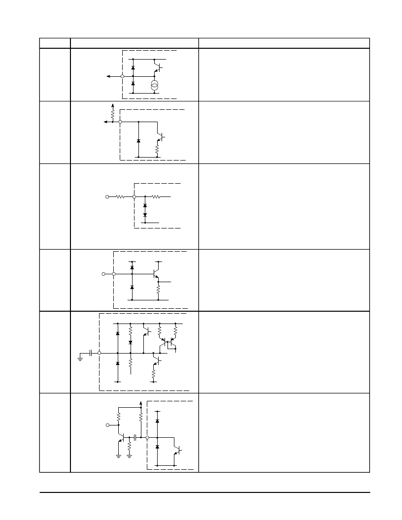
PIN FUNCTION DESCRIPTION (continued)
Pin
Description
Equivalent Internal Circuit
7
VCC
Gnd
To Vertical
Deflection
Amplifier
300
μ
A
Vertical Drive
The sawtooth derived on Pin 6 is used to drive an external power
amplifier vertical output stage. The amplitude, linearity and position of
the output ramp are adjustable via the MCU.
8
Gnd
To E–W
Amplifier
500
Parabola (E–W) Drive
An inverted parabolic waveform derived by squaring the vertical ramp
is used to drive an external power amplifier. In sets fitted with a diode
modulator type line output stage, this provides width control and
pin–cushion correction. The parabola is squared again to give a fourth
order correction term required for flat square tubes. The E–W
amplitude, dc level, tilt and corner correction are all adjustable by
means of the MCU. This is a current output and may be used, for
example, to drive the virtual ground of an external power amplifier
9
Gnd
Anode
Current
50 k
560 k
Anode Current
Used as an anode current monitor whose purpose is to: (1) Provide
E.H.T. compensation (anti–breathing) for the vertical ramp; and (2)
provide warning of excessive and overload beam current conditions.
The pin is connected via about 560 k
series resistor to the bottom of
the E.H.T. overwinding. Therefore, increasing beam current will pull
the voltage on this pin more negative. This change is sensed within
the chip and used to apply a correction to the ramp and parabola
amplitudes. With large beam currents, thresholds at +Vbe and
–2.0 Vbe set off warning flags to the MCU, which then has to take the
appropriate action. The anode current levels at which these
thresholds are reached are set up using fixed external resistors.
10
VCC
Gnd
Analog
Contrast
2.0 k
VCC
Anode Contrast
This pin is used as an Analog Contrast monitor, allowing fast Beam
Current Limiting (BCL). The fast BCL is controlled by Pin 10 voltage,
which decreases with the contrast reduction (see typical curve).
Above 2.5 V on the pin, the contrast remains maximum. Below 2.5,
the contrast is reduced by about 12 dB, which is reached at about
1.0 V.
11
100 nF
Gnd
200 k
200 k
10 k
Gnd
10 k
10 k
VCC
SECAM Calibration Loop
This pin is used for the storage capacitor of the analog SECAM
calibration loop (typically 100 nF). The capacitor is required
regardless of whether or not SECAM will be decoded.
12
VCC
18 k
1.0 k
47 k
0.0047
To Line O/P
Driver Stage
5.0 V
Horizontal Drive Output
Horizontal drive pulses having an approximately even mark–to–space
ratio emerge from this pin. This is an open–collector output which can
sink up to 10 mA. However, taking this much current is not
recommended since there is no separate ground pin available which
may be connected near the line output stage; noise could be injected
into the signal ground on the IC. Therefore, with a transformer driven
line output stage, this output has been designed to be used with an
extra external transistor inverter between the IC and the line driver.
The transistor is open during the period when the line deflection
transistor should be conducting.
相關(guān)PDF資料 |
PDF描述 |
|---|---|
| MC44035FTB | MULTISTANDARD VIDEO SIGNAL PROCESSOR WITH INTEGRATED CHROMA DELAY LINE |
| MC44030FTB | MULTISTANDARD VIDEO SIGNAL PROCESSOR WITH INTEGRATED CHROMA DELAY LINE |
| MC44030P | MULTISTANDARD VIDEO SIGNAL PROCESSOR WITH INTEGRATED CHROMA DELAY LINE |
| MC44035P | MULTISTANDARD VIDEO SIGNAL PROCESSOR WITH INTEGRATED CHROMA DELAY LINE |
| MC44107 | IR Remote Control Transmitter |
相關(guān)代理商/技術(shù)參數(shù) |
參數(shù)描述 |
|---|---|
| MC44007P | 制造商:MOTOROLA 制造商全稱:Motorola, Inc 功能描述:CHROMA 4 VIDEO PROCESSOR |
| MC4401 | 制造商:SHENZHENFREESCALE 制造商全稱:ShenZhen FreesCale Electronics. Co., Ltd 功能描述:P-Channel 30-V (D-S) MOSFET Low thermal impedance |
| MC44011 | 制造商:MOTOROLA 制造商全稱:Motorola, Inc 功能描述:Chroma 4 Multistandard Video Processor |
| MC44011FB | 制造商:MOTOROLA 制造商全稱:Motorola, Inc 功能描述:BUS CONTROLLED MULTISTANDARD VIDEO PROCESSOR |
| MC44011FN | 制造商:MOTOROLA 制造商全稱:Motorola, Inc 功能描述:Chroma 4 Multistandard Video Processor |
發(fā)布緊急采購(gòu),3分鐘左右您將得到回復(fù)。