- 您現(xiàn)在的位置:買賣IC網(wǎng) > PDF目錄371063 > MC74HC173N (MOTOROLA INC) Quad 3-State D Flip-Flop with Common Clock and Reset PDF資料下載
參數(shù)資料
| 型號: | MC74HC173N |
| 廠商: | MOTOROLA INC |
| 元件分類: | 通用總線功能 |
| 英文描述: | Quad 3-State D Flip-Flop with Common Clock and Reset |
| 中文描述: | HC/UH SERIES, POSITIVE EDGE TRIGGERED D FLIP-FLOP, TRUE OUTPUT, PDIP16 |
| 封裝: | PLASTIC, DIP-16 |
| 文件頁數(shù): | 4/6頁 |
| 文件大小: | 225K |
| 代理商: | MC74HC173N |
MC74HC173
MOTOROLA
High–Speed CMOS Logic Data
DL129 — Rev 6
4
PIN DESCRIPTIONS
INPUTS
D0, D1, D2, D3 (Pins 14, 13, 12, 11)
4–bit data inputs. Data on these pins, when enabled by the
Data–Enable Controls, are entered into the flip–flops on the
rising edge of the clock.
CLOCK (Pin 7)
Clock input.
OUTPUTS
Q0, Q1, Q2, Q3 (Pins 3, 4, 5, 6)
3–state register outputs. During normal operation of the
device, the outputs of the D flip–flops appear at these pins.
During 3–state operation, these outputs assume a high–
impedance state.
CONTROL INPUT
Reset (Pin 15)
Asynchronous reset input. A high level on this pin resets all
flip–flops and forces the Q outputs low, if they are not already
in high–impedance state.
DE1, DE2 (Pins 9, 10)
Active–low Data Enable Control inputs. When both Data
Enable Controls are low, data at the D inputs are loaded into
the flip–flops with the rising edge of the Clock input. When
either or both of these controls are high, there is no change in
the state of the flip–flops, regardless of any changes at the D
or Clock inputs.
OE1, OE2 (Pins 1, 2)
Output Enable Control inputs. When either or both of the
Output Enable Controls are high, the Q outputs of the device
are in the high–impedance state. When both controls are
low, the device outputs display the data in the flip–flops.
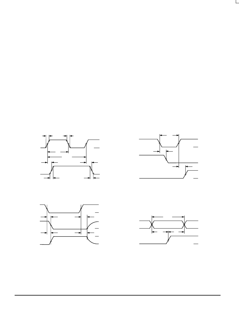
SWITCHING WAVEFORMS
tr
tf
VCC
GND
tTHL
tTLH
90%
50%
10%
90%
50%
10%
CLOCK
tPLH
tPHL
tw
50%
tPHL
VCC
GND
VCC
GND
CLOCK
RESET
50%
50%
trec
Figure 1.
Figure 2.
Q
Q
VCC
GND
VCC
GND
50%
50%
CLOCK
INPUT D
OR DE
50%
50%
50%
OE
Q
Q
tPZL
tPLZ
tPZH
tPHZ
10%
90%
VCC
GND
HIGH
IMPEDANCE
VOL
VOH
Figure 3.
Figure 4.
tw
1/fmax
HIGH
IMPEDANCE
VALID
tsu
th
相關PDF資料 |
PDF描述 |
|---|---|
| MC74HC174AD | Hex D Flip-Flop witth Common Clock and Reset |
| MC74HC174AN | Hex D Flip-Flop witth Common Clock and Reset |
| MC74HC194N | 4-Bit Bidirectional Universal Shift Register |
| MC74HC194 | 4-Bit Bidirectional Universal Shift Register |
| MC74HC195N | 4-Bit Universal Shift Register |
相關代理商/技術參數(shù) |
參數(shù)描述 |
|---|---|
| MC74HC174AD | 功能描述:觸發(fā)器 2-6V CMOS Hex RoHS:否 制造商:Texas Instruments 電路數(shù)量:2 邏輯系列:SN74 邏輯類型:D-Type Flip-Flop 極性:Inverting, Non-Inverting 輸入類型:CMOS 輸出類型: 傳播延遲時間:4.4 ns 高電平輸出電流:- 16 mA 低電平輸出電流:16 mA 電源電壓-最大:5.5 V 最大工作溫度:+ 85 C 安裝風格:SMD/SMT 封裝 / 箱體:X2SON-8 封裝:Reel |
| MC74HC174ADG | 功能描述:觸發(fā)器 2-6V CMOS Hex D-Type w/Clock RoHS:否 制造商:Texas Instruments 電路數(shù)量:2 邏輯系列:SN74 邏輯類型:D-Type Flip-Flop 極性:Inverting, Non-Inverting 輸入類型:CMOS 輸出類型: 傳播延遲時間:4.4 ns 高電平輸出電流:- 16 mA 低電平輸出電流:16 mA 電源電壓-最大:5.5 V 最大工作溫度:+ 85 C 安裝風格:SMD/SMT 封裝 / 箱體:X2SON-8 封裝:Reel |
| MC74HC174ADR2 | 功能描述:觸發(fā)器 2-6V CMOS Hex RoHS:否 制造商:Texas Instruments 電路數(shù)量:2 邏輯系列:SN74 邏輯類型:D-Type Flip-Flop 極性:Inverting, Non-Inverting 輸入類型:CMOS 輸出類型: 傳播延遲時間:4.4 ns 高電平輸出電流:- 16 mA 低電平輸出電流:16 mA 電源電壓-最大:5.5 V 最大工作溫度:+ 85 C 安裝風格:SMD/SMT 封裝 / 箱體:X2SON-8 封裝:Reel |
| MC74HC174ADR2G | 功能描述:觸發(fā)器 2-6V CMOS Hex D-Type w/Clock RoHS:否 制造商:Texas Instruments 電路數(shù)量:2 邏輯系列:SN74 邏輯類型:D-Type Flip-Flop 極性:Inverting, Non-Inverting 輸入類型:CMOS 輸出類型: 傳播延遲時間:4.4 ns 高電平輸出電流:- 16 mA 低電平輸出電流:16 mA 電源電壓-最大:5.5 V 最大工作溫度:+ 85 C 安裝風格:SMD/SMT 封裝 / 箱體:X2SON-8 封裝:Reel |
| MC74HC174ADT | 制造商:Rochester Electronics LLC 功能描述:- Bulk |
發(fā)布緊急采購,3分鐘左右您將得到回復。