- 您現在的位置:買賣IC網 > PDF目錄371036 > MC74HC254A (Motorola, Inc.) Octal 3-State Noninverting Buffer Transceiver PDF資料下載
參數資料
| 型號: | MC74HC254A |
| 廠商: | Motorola, Inc. |
| 英文描述: | Octal 3-State Noninverting Buffer Transceiver |
| 中文描述: | 八路三態收發器同相緩沖 |
| 文件頁數: | 2/7頁 |
| 文件大小: | 149K |
| 代理商: | MC74HC254A |
MC54/74HC245A
MOTOROLA
High–Speed CMOS Logic Data
DL129 — Rev 6
2
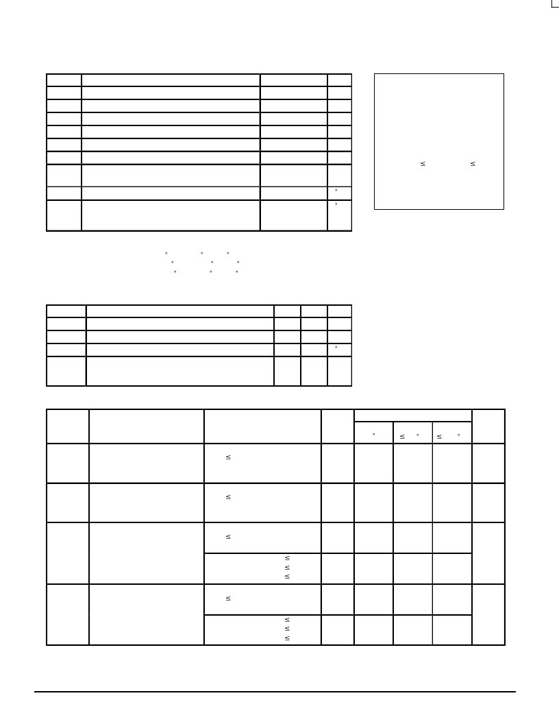
* Maximum Ratings are those values beyond which damage to the device may occur.
Functional operation should be restricted to the Recommended Operating Conditions.
Derating — Plastic DIP: – 10 mW/ C from 65 to 125 C
Ceramic DIP: – 10 mW/ C from 100 to 125 C
SOIC Package: – 7 mW/ C from 65 to 125 C
For high frequency or heavy load considerations, see Chapter 2 of the Motorola High–Speed CMOS Data Book (DL129/D).
ICC
PD
– 0.5 to VCC + 0.5
– 0.5 to VCC + 0.5
±
35
±
75
DC Output Voltage (Referenced to GND)
V
DC Output Current, per Pin
DC Supply Current, VCC and GND Pins
Power Dissipation in Still Air,Plastic or Ceramic DIP
mA
mA
750
mW
(Plastic DIP or SOIC Package)
Lead Temperature, 1 mm from Case for 10 Seconds
(Ceramic DIP)
260
300
RECOMMENDED OPERATING CONDITIONS
Symbol
VCC
Vin, Vout
Parameter
Min
2.0
Max
6.0
Unit
V
DC Input Voltage, Output Voltage (Referenced to GND)
DC Supply Voltage (Referenced to GND)
0
VCC
V
(Figure 1)
VCC = 2.0 V
0
1000
500
400
ns
3.15
4.2
4.2
25 C
1.5
1.5
3.15
4.2
Voltage
Symbol
VIH
|Iout|
20
μ
A
Parameter
Test Conditions
4.5
6.0
V
1.35
3.98
5.48
3.15
1.5
V
Minimum High–Level Input
Voltage
Vout = VCC – 0.1 V
|Iout|
20
μ
A
2.0
Maximum Low–Level Input
Voltage
4.5
6.0
Vout = 0.1 V
20
μ
A
4.5
4.4
5.9
0.1
4.4
5.9
1.35
1.35
V
Minimum High–Level Output
2.4 mA
Vin = VIH
0.26
0.26
4.4
5.9
V
Vin = VIH
|Iout|
|Iout|
6.0
3.0
6.0
6.0
0.1
0.4
5.34
5.2
VOL
Maximum Low–Level Output
Voltage
Vin = VIL
|Iout|
20
μ
A
2.0
0.1
0.1
0.1
0.4
0.1
V
|Iout|
0.33
This device contains protection
circuitry to guard against damage
due to high static voltages or electric
fields. However, precautions must
be taken to avoid applications of any
voltage higher than maximum rated
voltages to this high–impedance cir-
cuit. For proper operation, Vin and
Vout should be constrained to the
range GND
(Vin or Vout)
Unused inputs must always be
tied to an appropriate logic voltage
level (e.g., either GND or VCC).
Unused outputs must be left open.
VCC.
相關PDF資料 |
PDF描述 |
|---|---|
| MC54-74HC259A | 8-Bit Addressable Latch 1-of-8 Decoder |
| MC74HC259A | 8-Bit Addressable Latch 1-of-8 Decoder |
| MC74HC259AD | 8-Bit Addressable Latch 1-of-8 Decoder |
| MC74HC259ADT | 8-Bit Addressable Latch 1-of-8 Decoder |
| MC74HC259AN | 8-Bit Addressable Latch 1-of-8 Decoder |
相關代理商/技術參數 |
參數描述 |
|---|---|
| MC74HC257D | 制造商:Motorola Inc 功能描述: |
| MC74HC257DR2 | 制造商:Motorola 功能描述:74HC257 |
| MC74HC257FR2 | 制造商:Rochester Electronics LLC 功能描述:- Bulk |
| MC74HC257N | 制造商:Motorola Inc 功能描述: |
| MC74HC257ND | 制造商:Motorola Inc 功能描述: |
發布緊急采購,3分鐘左右您將得到回復。