- 您現(xiàn)在的位置:買賣IC網(wǎng) > PDF目錄371135 > MPC992 (Motorola, Inc.) Low Voltage PLL Clock Driver(低壓PLL時鐘驅(qū)動器) PDF資料下載
參數(shù)資料
| 型號: | MPC992 |
| 廠商: | Motorola, Inc. |
| 英文描述: | Low Voltage PLL Clock Driver(低壓PLL時鐘驅(qū)動器) |
| 中文描述: | 低電壓PLL時鐘驅(qū)動器(低壓鎖相環(huán)時鐘驅(qū)動器) |
| 文件頁數(shù): | 1/8頁 |
| 文件大小: | 104K |
| 代理商: | MPC992 |
SEMICONDUCTOR TECHNICAL DATA
1
REV 1
Motorola, Inc. 1996
7/96
The MPC992 is a 3.3V compatible, PLL based PECL clock generator
and distributor. The fully differential design ensures optimum skew and
PLL jitter performance. The performance of the device makes the
MPC992 ideal for workstations, main frame computer, telecommunication
and instrumentation applications. The device offers a crystal oscillator or
a differential PECL reference clock input to provide flexibility in the
reference clock interface. All of the control signals to the MPC992 are
LVTTL compatible inputs.
Fully Integrated PLL
Output Frequency of up to 400MHz
PECL Clock Inputs and Outputs
Operates from a 3.3V VCC Supply
Output Frequency Configurable
32 TQFP Packaging
±
25ps Cycle–Cycle Jitter
The MPC992 offers two banks of outputs which can be configured into
four different relationships. The output banks can be configured into 2:1,
3:1, 3:2 and 5:2 ratios to provide a wide variety of potential frequency
outputs. In addition to these two banks of outputs a synchronization output is also offered. The SYNC output will provide
information as to the time when the two output banks will transition positively in phase. This information can be important when
the odd ratios are used as it provides for a baseline point in the system timing. The SYNC output will pulse high for one Qa clock
period, centered on the rising Qa clock edge four edges prior to the Qb synchronous edge. The relationship is illustrated in the
timing diagrams in the data sheet.
The MPC992 offers several features to aid in system debug and test. The PECL reference input pins can be interfaced to a test
signal and the PLL can be bypassed to allow the designer to drive the MPC992 outputs directly. This allows for single stepping in
a system functional debug mode. In addition an overriding reset is provided which will force all of the Q outputs LOW upon
assertion.
The MPC992 is packaged in a 32–lead TQFP package to optimize both performance and board density.
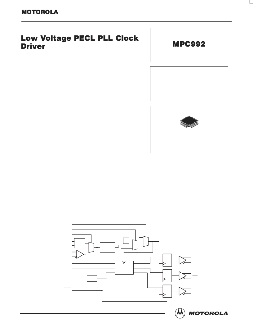
Qan
Qan
(x4)
Qbn
Qbn
(x3)
SYNC
SYNC
(x1)
Frequency
Generator
PLL_EN
VCO_SEL
PECL_CLK
PECL_CLK
XTAL_SEL
XTAL
OSC
XTAL1
XTAL2
Integrated
PLL
x2
FSEL0
FSEL1
POR
Reset
MPC992 LOGIC DIAGRAM
1
0
0
1
0
1
LOW VOLTAGE
PLL CLOCK DRIVER
FA SUFFIX
PLASTIC TQFP PACKAGE
CASE 873A-02
相關(guān)PDF資料 |
PDF描述 |
|---|---|
| MPC993 | Dynamic Switch PLL Clock Driver(動態(tài)開關(guān)PLL時鐘驅(qū)動器) |
| MPC9990 | Low Voltage PLL Clock Driver(低壓PLL時鐘驅(qū)動器) |
| MPF102 | JFET VHF Amplifier |
| MPF102 | JFET VHF Amplifier |
| MPF102 | N-Channel RF Amplifier |
相關(guān)代理商/技術(shù)參數(shù) |
參數(shù)描述 |
|---|---|
| MPC992D33 F44A WAF | 制造商:Motorola Inc 功能描述: |
| MPC993 | 制造商:MOTOROLA 制造商全稱:Motorola, Inc 功能描述:Dynamic Switch PLL Clock Driver |
| MPC9992 | 制造商:MOTOROLA 制造商全稱:Motorola, Inc 功能描述:3.3 DIFFRERENTIAL ECL/PECL PLL CLOCK GENERATOR |
| MPC9992AC | 功能描述:時鐘發(fā)生器及支持產(chǎn)品 RoHS:否 制造商:Silicon Labs 類型:Clock Generators 最大輸入頻率:14.318 MHz 最大輸出頻率:166 MHz 輸出端數(shù)量:16 占空比 - 最大:55 % 工作電源電壓:3.3 V 工作電源電流:1 mA 最大工作溫度:+ 85 C 安裝風(fēng)格:SMD/SMT 封裝 / 箱體:QFN-56 |
| MPC9992ACR2 | 功能描述:時鐘發(fā)生器及支持產(chǎn)品 RoHS:否 制造商:Silicon Labs 類型:Clock Generators 最大輸入頻率:14.318 MHz 最大輸出頻率:166 MHz 輸出端數(shù)量:16 占空比 - 最大:55 % 工作電源電壓:3.3 V 工作電源電流:1 mA 最大工作溫度:+ 85 C 安裝風(fēng)格:SMD/SMT 封裝 / 箱體:QFN-56 |
發(fā)布緊急采購,3分鐘左右您將得到回復(fù)。