- 您現(xiàn)在的位置:買賣IC網(wǎng) > PDF目錄382345 > MPF4393G (ON SEMICONDUCTOR) JFET Switching Transistors N−Channel − Depletion PDF資料下載
參數(shù)資料
| 型號: | MPF4393G |
| 廠商: | ON SEMICONDUCTOR |
| 元件分類: | 功率晶體管 |
| 英文描述: | JFET Switching Transistors N−Channel − Depletion |
| 中文描述: | 30 V, N-CHANNEL, Si, SMALL SIGNAL, JFET, TO-92 |
| 封裝: | CASE 29-11, TO-226AA, 3 PIN |
| 文件頁數(shù): | 4/6頁 |
| 文件大小: | 83K |
| 代理商: | MPF4393G |
MPF4392, MPF4393
http://onsemi.com
4
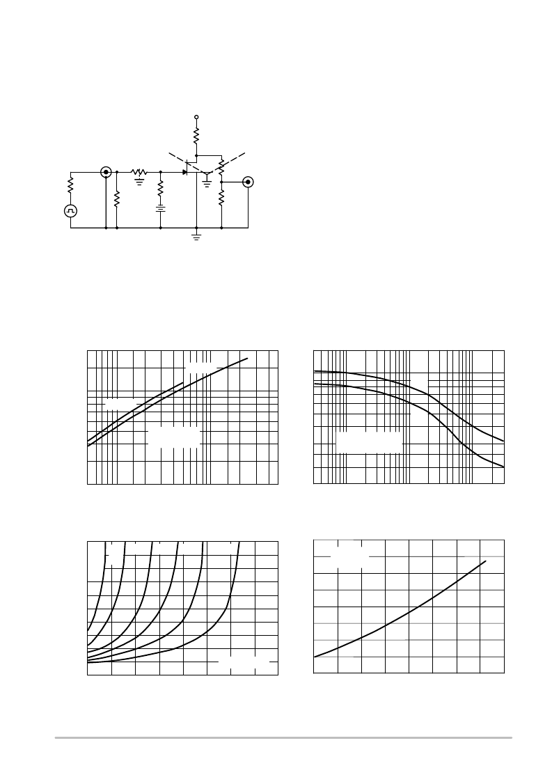
Figure 5. Switching Time Test Circuit
10
2.0
15
3.0
5.0
7.0
0.5
1.0
3.0
30
5.0
0.3
0.1
10
0.05
0.03
V
R
, REVERSE VOLTAGE (VOLTS)
C
50
170
20
10
40
80
140
70
r
1.8
1.0
2.0
1.2
1.4
1.6
0.8
0.6
0.4
,
d
R
T
channel
, CHANNEL TEMPERATURE (
°
C)
1.5
1.0
110
V
DD
V
GG
R
GG
R
T
R
GEN
50
V
GEN
R
K
R
D
OUTPUT
INPUT
50
50
SET V
DS(off)
= 10 V
INPUT PULSE
t
r
≤
0.25 ns
t
f
≤
0.5 ns
PULSE WIDTH = 2.0 s
DUTY CYCLE
≤
2.0%
R
GG
R
K
R
D
′
= R
D
(R
T
+ 50)
R
D
+ R
T
+ 50
Figure 6. Typical Forward Transfer Admittance
NOTE 1
The switching characteristics shown above were measured using a
test circuit similar to Figure 5. At the beginning of the switching
interval, the gate voltage is at Gate Supply Voltage (V
GG
). The
DrainSource Voltage (V
DS
) is slightly lower than Drain Supply
Voltage (V
DD
) due to the voltage divider. Thus Reverse Transfer
Capacitance (C
rss
) or GateDrain Capacitance (C
gd
) is charged to
V
GG
+ V
DS
.
During the turnon interval, GateSource Capacitance (C
gs
)
discharges through the series combination of R
Gen
and R
K
. C
gd
must discharge to V
DS(on)
through R
G
and R
K
in series with the
parallel combination of effective load impedance (R
′
D
) and
DrainSource Resistance (r
ds
). During the turnoff, this charge
flow is reversed.
Predicting turnon time is somewhat difficult as the channel
resistance r
ds
is a function of the gatesource voltage. While C
gs
discharges, V
GS
approaches zero and r
ds
decreases. Since C
gd
discharges through r
ds
, turnon time is nonlinear. During turnoff,
the situation is reversed with r
ds
increasing as C
gd
charges.
The above switching curves show two impedance conditions:
1) R
K
is equal to R
D
′
which simulates the switching behavior of
cascaded stages where the driving source impedance is normally the
load impedance of the previous stage, and 2) R
K
= 0 (low
impedance) the driving source impedance is that of the generator.
Figure 7. Typical Capacitance
I
D
, DRAIN CURRENT (mA)
2.0
5.0
3.0
7.0
0.5
1.0
3.0
7.0
5.0
50
30
10
20
0.7
2.0
10
20
,
f
y
80
120
160
200
1.0
3.0
5.0
2.0
V
GS
, GATESOURCE VOLTAGE (VOLTS)
4.0
0
40
6.0
7.0
8.0
0
r
,
d
R
T
channel
= 25
°
C
(C
ds
IS NEGLIGIBLE)
C
gs
T
channel
= 25
°
C
V
DS
= 15 V
Figure 8. Effect of GateSource Voltage
On DrainSource Resistance
Figure 9. Effect of Temperature On
DrainSource OnState Resistance
MPF4392
MPF4393
C
gd
I
D
= 1.0 mA
V
GS
= 0
I
DSS
= 10
mA
25
mA
50 mA
75 mA 100 mA
125 mA
T
channel
= 25
°
C
相關(guān)PDF資料 |
PDF描述 |
|---|---|
| MPF4393RLRP | JFET Switching Transistors N−Channel − Depletion |
| MPF4393RLRPG | JFET Switching Transistors N−Channel − Depletion |
| MPM3002 | TMOS ICePAK Power Module |
| MPM3003 | ICE PAK POWER MODULE |
| MPN3404 | SILICON PIN SWITCHING DIODE |
相關(guān)代理商/技術(shù)參數(shù) |
參數(shù)描述 |
|---|---|
| MPF4393RLRP | 功能描述:JFET 30V 10mA RoHS:否 制造商:ON Semiconductor 晶體管極性:N-Channel 漏極電流(Vgs=0 時的 Idss):50 mA 漏源電壓 VDS:15 V 閘/源擊穿電壓: 漏極連續(xù)電流:50 mA 配置: 安裝風(fēng)格: 封裝 / 箱體:SC-59 封裝:Reel |
| MPF4393RLRP WAF | 制造商:ON Semiconductor 功能描述: |
| MPF4393RLRPG | 功能描述:JFET 30V 10mA RoHS:否 制造商:ON Semiconductor 晶體管極性:N-Channel 漏極電流(Vgs=0 時的 Idss):50 mA 漏源電壓 VDS:15 V 閘/源擊穿電壓: 漏極連續(xù)電流:50 mA 配置: 安裝風(fēng)格: 封裝 / 箱體:SC-59 封裝:Reel |
| MPF480D4 | 功能描述:固態(tài)繼電器-PCB安裝 Obsolete use MCX480D5 RoHS:否 制造商:Omron Electronics 控制電壓范圍: 負(fù)載電壓額定值:40 V 負(fù)載電流額定值:120 mA 觸點形式:1 Form A (SPST-NO) 輸出設(shè)備:MOSFET 封裝 / 箱體:USOP-4 安裝風(fēng)格:SMD/SMT |
| MPF4856RLRA | 制造商:Rochester Electronics LLC 功能描述:- Bulk 制造商:Motorola Inc 功能描述: 制造商:MOTOROLA 功能描述: |
發(fā)布緊急采購,3分鐘左右您將得到回復(fù)。