- 您現在的位置:買賣IC網 > PDF目錄382346 > MPSA70RLRMG (ON SEMICONDUCTOR) Amplifier Transistor PNP Silicon PDF資料下載
參數資料
| 型號: | MPSA70RLRMG |
| 廠商: | ON SEMICONDUCTOR |
| 元件分類: | 功率晶體管 |
| 英文描述: | Amplifier Transistor PNP Silicon |
| 中文描述: | 100 mA, 40 V, PNP, Si, SMALL SIGNAL TRANSISTOR, TO-92 |
| 封裝: | PLASTIC, TO-226AA, 3 PIN |
| 文件頁數: | 6/7頁 |
| 文件大小: | 112K |
| 代理商: | MPSA70RLRMG |
MPSA70
http://onsemi.com
6
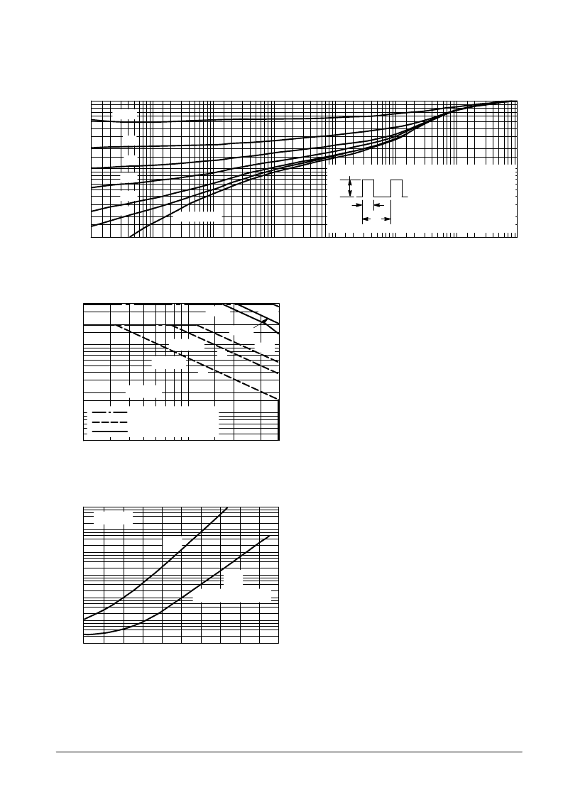
Figure 17. Thermal Response
t, TIME (ms)
1.0
0.7
0.01
r
(
0.01
0.02
0.03
0.05
0.07
0.1
0.2
0.3
0.5
0.02
0.05
0.1
0.2
0.5
1.0
2.0
5.0
10
20
50
100
200
500
1.0k 2.0k
5.0k 10k
20k
50k
100k
D = 0.5
0.2
0.1
0.05
0.02
0.01
SINGLE PULSE
DUTY CYCLE, D = t
1
/t
2
D CURVES APPLY FOR POWER
PULSE TRAIN SHOWN
READ TIME AT t
1
(SEE AN569)
Z
JA(t)
= r(t)
R
JA
T
J(pk)
T
A
= P
(pk)
Z
JA(t)
t
1
t
2
P
(pk)
FIGURE 18
Figure 19. ActiveRegion Safe Operating Area
T
J
, JUNCTION TEMPERATURE (
°
C)
10
4
4
0
I
Figure 20. Typical Collector Leakage Current
V
CE
, COLLECTOREMITTER VOLTAGE (VOLTS)
400
2.0
I
DESIGN NOTE: USE OF THERMAL RESPONSE DATA
A train of periodical power pulses can be represented by the
model as shown in Figure 19. Using the model and the device
thermal response the normalized effective transient thermal
resistance of Figure 17 was calculated for various duty cycles.
To find Z
JA(t)
, multiply the value obtained from Figure 17 by
the steady state value R
JA
.
Example:
Dissipating 2.0 watts peak under the following conditions:
t
1
= 1.0 ms, t
2
= 5.0 ms (D = 0.2)
Using Figure 17 at a pulse width of 1.0 ms and D = 0.2, the
reading of r(t) is 0.22.
The peak rise in junction temperature is therefore
T = r(t) x P
(pk)
x R
JA
= 0.22 x 2.0 x 200 = 88
°
C.
For more information, see AN569/D.
The safe operating area curves indicate I
C
V
CE
limits of the
transistor that must be observed for reliable operation. Collector
load lines for specific circuits must fall below the limits indicated
by the applicable curve.
The data of Figure 18 is based upon T
J(pk)
= 150
°
C; T
C
or T
A
is variable depending upon conditions. Pulse curves are valid for
duty cycles to 10% provided T
J(pk)
≤
150
°
C. T
J(pk)
may be
calculated from the data in Figure 17. At high case or ambient
temperatures, thermal limitations will reduce the power than can
be handled to values less than the limitations imposed by second
breakdown.
10
2
10
1
10
0
10
1
10
2
10
3
2
0
0
+20
+40
+60
+80 +100 +120 +140 +160
V
CC
= 30 V
I
CEO
I
CBO
AND
I
CEX
@ V
BE(off)
= 3.0 V
T
A
= 25
°
C
CURRENT LIMIT
THERMAL LIMIT
SECOND BREAKDOWN LIMIT
1.0 ms
10 s
T
C
= 25
°
C
1.0 s
dc
dc
4.0
6.0
10
20
40
60
100
200
4.0
6.0
8.0 10
20
40
T
J
= 150
°
C
100 s
相關PDF資料 |
PDF描述 |
|---|---|
| MPSW45AG | One Watt Darlington Transistors NPN Silicon |
| MPSW45ARLRA | One Watt Darlington Transistors NPN Silicon |
| MPSW45ARLRAG | One Watt Darlington Transistors NPN Silicon |
| MPSW45AZL1 | One Watt Darlington Transistors NPN Silicon |
| MPSW45AZL1G | One Watt Darlington Transistors NPN Silicon |
相關代理商/技術參數 |
參數描述 |
|---|---|
| MPSA75 | 制造商:CENTRAL 制造商全稱:Central Semiconductor Corp 功能描述:Small Signal Transistors |
| MPSA75_06 | 制造商:ONSEMI 制造商全稱:ON Semiconductor 功能描述:Darlington Transistors PNP Silicon |
| MPSA75RLRA | 功能描述:達林頓晶體管 500mA 40V PNP RoHS:否 制造商:Texas Instruments 配置:Octal 晶體管極性:NPN 集電極—發射極最大電壓 VCEO:50 V 發射極 - 基極電壓 VEBO: 集電極—基極電壓 VCBO: 最大直流電集電極電流:0.5 A 最大集電極截止電流: 功率耗散: 最大工作溫度:+ 150 C 安裝風格:SMD/SMT 封裝 / 箱體:SOIC-18 封裝:Reel |
| MPSA75RLRAG | 功能描述:達林頓晶體管 500mA 40V PNP RoHS:否 制造商:Texas Instruments 配置:Octal 晶體管極性:NPN 集電極—發射極最大電壓 VCEO:50 V 發射極 - 基極電壓 VEBO: 集電極—基極電壓 VCBO: 最大直流電集電極電流:0.5 A 最大集電極截止電流: 功率耗散: 最大工作溫度:+ 150 C 安裝風格:SMD/SMT 封裝 / 箱體:SOIC-18 封裝:Reel |
| MPSA75RLRP | 功能描述:達林頓晶體管 500mA 40V PNP RoHS:否 制造商:Texas Instruments 配置:Octal 晶體管極性:NPN 集電極—發射極最大電壓 VCEO:50 V 發射極 - 基極電壓 VEBO: 集電極—基極電壓 VCBO: 最大直流電集電極電流:0.5 A 最大集電極截止電流: 功率耗散: 最大工作溫度:+ 150 C 安裝風格:SMD/SMT 封裝 / 箱體:SOIC-18 封裝:Reel |
發布緊急采購,3分鐘左右您將得到回復。