- 您現在的位置:買賣IC網 > PDF目錄98034 > MPSA93RL1 (ON SEMICONDUCTOR) 500 mA, 200 V, PNP, Si, SMALL SIGNAL TRANSISTOR, TO-92 PDF資料下載
參數資料
| 型號: | MPSA93RL1 |
| 廠商: | ON SEMICONDUCTOR |
| 元件分類: | 小信號晶體管 |
| 英文描述: | 500 mA, 200 V, PNP, Si, SMALL SIGNAL TRANSISTOR, TO-92 |
| 封裝: | PLASTIC, TO-226AA, 3 PIN |
| 文件頁數: | 34/34頁 |
| 文件大小: | 320K |
| 代理商: | MPSA93RL1 |
第1頁第2頁第3頁第4頁第5頁第6頁第7頁第8頁第9頁第10頁第11頁第12頁第13頁第14頁第15頁第16頁第17頁第18頁第19頁第20頁第21頁第22頁第23頁第24頁第25頁第26頁第27頁第28頁第29頁第30頁第31頁第32頁第33頁當前第34頁
Packaging Specifications
6–6
Motorola Small–Signal Transistors, FETs and Diodes Device Data
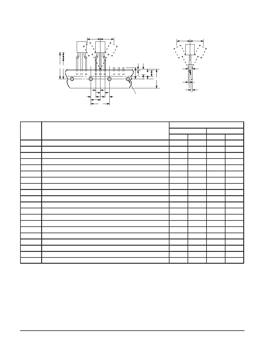
TO–92 EIA RADIAL TAPE IN FAN FOLD BOX OR ON REEL
H2A
H
F1
F2
P2
P1
P
D
W
W1
L1
W2
H2B
T1
T
T2
H4 H5
H1
Figure 1. Device Positioning on Tape
L
Specification
Inches
Millimeter
Symbol
Item
Min
Max
Min
Max
D
Tape Feedhole Diameter
0.1496
0.1653
3.8
4.2
D2
Component Lead Thickness Dimension
0.015
0.020
0.38
0.51
F1, F2
Component Lead Pitch
0.0945
0.110
2.4
2.8
H
Bottom of Component to Seating Plane
.059
.156
1.5
4.0
H1
Feedhole Location
0.3346
0.3741
8.5
9.5
H2A
Deflection Left or Right
0
0.039
0
1.0
H2B
Deflection Front or Rear
0
0.051
0
1.0
H4
Feedhole to Bottom of Component
0.7086
0.768
18
19.5
H5
Feedhole to Seating Plane
0.610
0.649
15.5
16.5
L
Defective Unit Clipped Dimension
0.3346
0.433
8.5
11
L1
Lead Wire Enclosure
0.09842
—
2.5
—
P
Feedhole Pitch
0.4921
0.5079
12.5
12.9
P1
Feedhole Center to Center Lead
0.2342
0.2658
5.95
6.75
P2
First Lead Spacing Dimension
0.1397
0.1556
3.55
3.95
T
Adhesive Tape Thickness
0.06
0.08
0.15
0.20
T1
Overall Taped Package Thickness
—
0.0567
—
1.44
T2
Carrier Strip Thickness
0.014
0.027
0.35
0.65
W
Carrier Strip Width
0.6889
0.7481
17.5
19
W1
Adhesive Tape Width
0.2165
0.2841
5.5
6.3
W2
Adhesive Tape Position
.0059
0.01968
.15
0.5
NOTES:
1. Maximum alignment deviation between leads not to be greater than 0.2 mm.
2. Defective components shall be clipped from the carrier tape such that the remaining protrusion (L) does not exceed a maximum of 11 mm.
3. Component lead to tape adhesion must meet the pull test requirements established in Figures 5, 6 and 7.
4. Maximum non–cumulative variation between tape feed holes shall not exceed 1 mm in 20 pitches.
5. Holddown tape not to extend beyond the edge(s) of carrier tape and there shall be no exposure of adhesive.
6. No more than 1 consecutive missing component is permitted.
7. A tape trailer and leader, having at least three feed holes is required before the first and after the last component.
8. Splices will not interfere with the sprocket feed holes.
相關PDF資料 |
PDF描述 |
|---|---|
| MPSH10L34Z | UHF BAND, Si, NPN, RF SMALL SIGNAL TRANSISTOR |
| MPSH10J18Z | UHF BAND, Si, NPN, RF SMALL SIGNAL TRANSISTOR |
| MPSH10D75Z | UHF BAND, Si, NPN, RF SMALL SIGNAL TRANSISTOR, TO-92 |
| MPSH10D27Z | UHF BAND, Si, NPN, RF SMALL SIGNAL TRANSISTOR, TO-92 |
| MMBTH10D87Z | UHF BAND, Si, NPN, RF SMALL SIGNAL TRANSISTOR |
相關代理商/技術參數 |
參數描述 |
|---|---|
| MPSA93RLRM | 功能描述:兩極晶體管 - BJT 500mA 200V PNP RoHS:否 制造商:STMicroelectronics 配置: 晶體管極性:PNP 集電極—基極電壓 VCBO: 集電極—發射極最大電壓 VCEO:- 40 V 發射極 - 基極電壓 VEBO:- 6 V 集電極—射極飽和電壓: 最大直流電集電極電流: 增益帶寬產品fT: 直流集電極/Base Gain hfe Min:100 A 最大工作溫度: 安裝風格:SMD/SMT 封裝 / 箱體:PowerFLAT 2 x 2 |
| MPSA93RLRMG | 功能描述:兩極晶體管 - BJT 500mA 200V PNP RoHS:否 制造商:STMicroelectronics 配置: 晶體管極性:PNP 集電極—基極電壓 VCBO: 集電極—發射極最大電壓 VCEO:- 40 V 發射極 - 基極電壓 VEBO:- 6 V 集電極—射極飽和電壓: 最大直流電集電極電流: 增益帶寬產品fT: 直流集電極/Base Gain hfe Min:100 A 最大工作溫度: 安裝風格:SMD/SMT 封裝 / 箱體:PowerFLAT 2 x 2 |
| MPSA93STOA | 功能描述:兩極晶體管 - BJT - RoHS:否 制造商:STMicroelectronics 配置: 晶體管極性:PNP 集電極—基極電壓 VCBO: 集電極—發射極最大電壓 VCEO:- 40 V 發射極 - 基極電壓 VEBO:- 6 V 集電極—射極飽和電壓: 最大直流電集電極電流: 增益帶寬產品fT: 直流集電極/Base Gain hfe Min:100 A 最大工作溫度: 安裝風格:SMD/SMT 封裝 / 箱體:PowerFLAT 2 x 2 |
| MPSA93STOB | 功能描述:兩極晶體管 - BJT - RoHS:否 制造商:STMicroelectronics 配置: 晶體管極性:PNP 集電極—基極電壓 VCBO: 集電極—發射極最大電壓 VCEO:- 40 V 發射極 - 基極電壓 VEBO:- 6 V 集電極—射極飽和電壓: 最大直流電集電極電流: 增益帶寬產品fT: 直流集電極/Base Gain hfe Min:100 A 最大工作溫度: 安裝風格:SMD/SMT 封裝 / 箱體:PowerFLAT 2 x 2 |
| MPSA93STZ | 功能描述:兩極晶體管 - BJT - RoHS:否 制造商:STMicroelectronics 配置: 晶體管極性:PNP 集電極—基極電壓 VCBO: 集電極—發射極最大電壓 VCEO:- 40 V 發射極 - 基極電壓 VEBO:- 6 V 集電極—射極飽和電壓: 最大直流電集電極電流: 增益帶寬產品fT: 直流集電極/Base Gain hfe Min:100 A 最大工作溫度: 安裝風格:SMD/SMT 封裝 / 箱體:PowerFLAT 2 x 2 |
發布緊急采購,3分鐘左右您將得到回復。