- 您現(xiàn)在的位置:買賣IC網(wǎng) > PDF目錄98048 > MUN5112T3 (ON SEMICONDUCTOR) 100 mA, 50 V, PNP, Si, SMALL SIGNAL TRANSISTOR PDF資料下載
參數(shù)資料
| 型號: | MUN5112T3 |
| 廠商: | ON SEMICONDUCTOR |
| 元件分類: | 小信號晶體管 |
| 英文描述: | 100 mA, 50 V, PNP, Si, SMALL SIGNAL TRANSISTOR |
| 封裝: | SC-70, 3 PIN |
| 文件頁數(shù): | 1/16頁 |
| 文件大小: | 136K |
| 代理商: | MUN5112T3 |
Semiconductor Components Industries, LLC, 2001
January, 2001 – Rev. 4
1
Publication Order Number:
MUN5111T1/D
MUN5111T1 Series
Preferred Devices
Bias Resistor Transistor
PNP Silicon Surface Mount Transistor
with Monolithic Bias Resistor Network
This new series of digital transistors is designed to replace a single
device and its external resistor bias network. The BRT (Bias Resistor
Transistor) contains a single transistor with a monolithic bias network
consisting of two resistors; a series base resistor and a base–emitter
resistor. The BRT eliminates these individual components by
integrating them into a single device. The use of a BRT can reduce
both system cost and board space. The device is housed in the
SC–70/SOT–323 package which is designed for low power surface
mount applications.
Simplifies Circuit Design
Reduces Board Space
Reduces Component Count
The SC–70/SOT–323 package can be soldered using wave or reflow.
The modified gull–winged leads absorb thermal stress during
soldering eliminating the possibility of damage to the die.
Available in 8 mm embossed tape and reel
Use the Device Number to order the 7 inch/3000 unit reel.
Replace “T1” with “T3” in the Device Number to order
the 13 inch/10,000 unit reel.
MAXIMUM RATINGS (TA = 25°C unless otherwise noted)
Rating
Symbol
Value
Unit
Collector-Base Voltage
VCBO
50
Vdc
Collector-Emitter Voltage
VCEO
50
Vdc
Collector Current
IC
100
mAdc
THERMAL CHARACTERISTICS
Characteristic
Symbol
Max
Unit
Total Device Dissipation
TA = 25°C
Derate above 25
°C
PD
202 (Note 1.)
310 (Note 2.)
1.6 (Note 1.)
2.5 (Note 2.)
mW
°C/W
Thermal Resistance –
Junction-to-Ambient
RθJA
618 (Note 1.)
403 (Note 2.)
°C/W
Thermal Resistance –
Junction-to-Lead
RθJL
280 (Note 1.)
332 (Note 2.)
°C/W
Junction and Storage
Temperature Range
TJ, Tstg
–55 to +150
°C
1. FR–4 @ Minimum Pad
2. FR–4 @ 1.0 x 1.0 inch Pad
http://onsemi.com
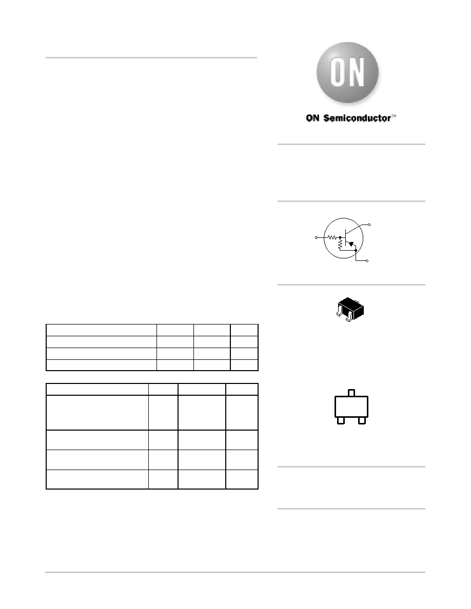
PNP SILICON
BIAS RESISTOR
TRANSISTORS
SC–70/SOT–323
CASE 419
STYLE 3
Preferred devices are recommended choices for future use
and best overall value.
3
2
1
PIN 3
COLLECTOR
(OUTPUT)
PIN 2
EMITTER
(GROUND)
PIN 1
BASE
(INPUT)
R1
R2
MARKING DIAGRAM
6x = Specific Device Code
x
= (See Marking Table)
M = Date Code
6x M
DEVICE MARKING INFORMATION
See specific marking information in the device marking table
on page 2 of this data sheet.
相關(guān)PDF資料 |
PDF描述 |
|---|---|
| MUN5137T3 | 100 mA, 50 V, PNP, Si, SMALL SIGNAL TRANSISTOR |
| MUN5135T3 | 100 mA, 50 V, PNP, Si, SMALL SIGNAL TRANSISTOR |
| MUN5130T3 | 100 mA, 50 V, PNP, Si, SMALL SIGNAL TRANSISTOR |
| MUN5111T3 | 100 mA, 50 V, PNP, Si, SMALL SIGNAL TRANSISTOR |
| MUN5115T3 | 100 mA, 50 V, PNP, Si, SMALL SIGNAL TRANSISTOR |
相關(guān)代理商/技術(shù)參數(shù) |
參數(shù)描述 |
|---|---|
| MUN5113 | 制造商:WEITRON 制造商全稱:Weitron Technology 功能描述:Bias Resistor Transistor PNP Silicon |
| MUN5113DW | 制造商:WEITRON 制造商全稱:Weitron Technology 功能描述:Dual Bias Resistor Transistor PNP Silicon |
| MUN5113DW1 | 制造商:ONSEMI 制造商全稱:ON Semiconductor 功能描述:Dual Bias Resistor Transistors |
| MUN5113DW1T1 | 功能描述:開關(guān)晶體管 - 偏壓電阻器 100mA 50V BRT Dual RoHS:否 制造商:ON Semiconductor 配置: 晶體管極性:NPN/PNP 典型輸入電阻器: 典型電阻器比率: 安裝風格:SMD/SMT 封裝 / 箱體: 直流集電極/Base Gain hfe Min:200 mA 最大工作頻率: 集電極—發(fā)射極最大電壓 VCEO:50 V 集電極連續(xù)電流:150 mA 峰值直流集電極電流: 功率耗散:200 mW 最大工作溫度: 封裝:Reel |
| MUN5113DW1T1G | 功能描述:開關(guān)晶體管 - 偏壓電阻器 SS BR XSTR PNP 50V RoHS:否 制造商:ON Semiconductor 配置: 晶體管極性:NPN/PNP 典型輸入電阻器: 典型電阻器比率: 安裝風格:SMD/SMT 封裝 / 箱體: 直流集電極/Base Gain hfe Min:200 mA 最大工作頻率: 集電極—發(fā)射極最大電壓 VCEO:50 V 集電極連續(xù)電流:150 mA 峰值直流集電極電流: 功率耗散:200 mW 最大工作溫度: 封裝:Reel |
發(fā)布緊急采購,3分鐘左右您將得到回復。