- 您現在的位置:買賣IC網 > PDF目錄361075 > NB4N441 (ON SEMICONDUCTOR) 3.3V Serial Input MultiProtocol PLL Clock Synthesizer, Differential LVPECL Output(3.3V串行輸入多協議PLL時鐘合成器, 差分LVPECL輸出) PDF資料下載
參數資料
| 型號: | NB4N441 |
| 廠商: | ON SEMICONDUCTOR |
| 英文描述: | 3.3V Serial Input MultiProtocol PLL Clock Synthesizer, Differential LVPECL Output(3.3V串行輸入多協議PLL時鐘合成器, 差分LVPECL輸出) |
| 中文描述: | 3.3串行輸入多協議PLL時鐘合成器,差分LVPECL輸出電壓(3.3V串行輸入多協議PLL的時鐘合成器,差分LVPECL的輸出) |
| 文件頁數: | 10/12頁 |
| 文件大小: | 168K |
| 代理商: | NB4N441 |
NB4N441
http://onsemi.com
10
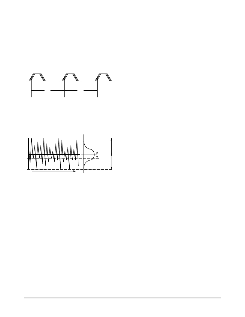
Jitter Performance
Jitter is a common parameter associated with clock
generation and distribution. Clock jitter can be defined as the
deviation in a clock’s output transition from its
ideal position.
Cycle
to
Cycle Jitter
(short
term) is the period
variation between two adjacent cycles over a defined
number of observed cycles. The number of cycles observed
is application dependent but the JEDEC specification is
1000 cycles.
Figure 8. Cycle
to
Cycle Jitter
T
JITTER(cycle
cycle)
= T
1
T
0
T
0
T
1
Peak
to
Peak Jitter
is the difference between the
highest and lowest acquired value and is represented as the
width of the Gaussian base.
Figure 9. Peak
to
Peak Jitter
Time
Typical
Gaussian
Distribution
RMS
or one
Sigma
Jitter
J
P
t
P
There are different ways to measure jitter and often they
are confused with one another. The typical method of
measuring jitter is to look at the timing signal with an
oscilloscope and observe the variations in period
to
period
or cycle
to
cycle. If the scope is set up to trigger on every
rising or falling edge, set to infinite persistence mode and
allowed to trace sufficient cycles, it is possible to determine
the maximum and minimum periods of the timing signal.
Digital scopes can accumulate a large number of cycles,
create a histogram of the edge placements and record
peak
to
peak as well as standard deviations of the jitter.
Care must be taken that the measured edge is the edge
immediately following the trigger edge. These scopes can
also store a finite number of period durations and
post
processing software can analyze the data to find the
maximum and minimum periods.
Recent hardware and software developments have
resulted in advanced jitter measurement techniques. The
Tektronix TDS
series oscilloscopes have superb jitter
analysis capabilities on non
contiguous clocks with their
histogram and statistics capabilities. The Tektronix
TDSJIT2/3 Jitter Analysis software provides many key
timing parameter measurements and will extend that
capability by making jitter measurements on contiguous
clock and data cycles from single
shot acquisitions.
M1 by Amherst was used as well and both test methods
correlated.
Long
Term Period Jitter
is the maximum jitter
observed at the end of a period’s edge when compared to the
position of the perfect reference clock’s edge and is specified
by the number of cycles over which the jitter is measured.
The number of cycles used to look for the maximum jitter
varies by application but the JEDEC spec is
10,000 observed cycles.
The NBC4N441 exhibit long term and cycle
to
cycle
jitter, which rivals that of SAW based oscillators. This jitter
performance comes with the added flexibility associated
with a synthesizer over a fixed frequency oscillator. The
jitter data presented should provide users with enough
information to determine the effect on their overall timing
budget. The jitter performance meets the needs of most
system designs while adding the flexibility of frequency
margining and field upgrades. These features are not
available with a fixed frequency SAW oscillator.
相關PDF資料 |
PDF描述 |
|---|---|
| NB4N840M | 3.3V 2.7Gb/s Dual Differential Clock/Data 2 x 2 Crosspoint Switch with CML Output and Internal Termination(帶CML輸出和內部終端的3.3V,2.7Gb/s雙差分時鐘/數據2x2交點開關) |
| NB6L11 | 2.5V / 3.3V MULTILEVEL INPUT TO DIFFERENTIAL LVPECL/LVNECL 1:2 CLOCK OR DATA FANOUT BUFFER / TRANSLATOR |
| NB6L11D | 2.5V / 3.3V MULTILEVEL INPUT TO DIFFERENTIAL LVPECL/LVNECL 1:2 CLOCK OR DATA FANOUT BUFFER / TRANSLATOR |
| NB6L11DR2 | 2.5V / 3.3V MULTILEVEL INPUT TO DIFFERENTIAL LVPECL/LVNECL 1:2 CLOCK OR DATA FANOUT BUFFER / TRANSLATOR |
| NB6L11DT | 2.5V / 3.3V MULTILEVEL INPUT TO DIFFERENTIAL LVPECL/LVNECL 1:2 CLOCK OR DATA FANOUT BUFFER / TRANSLATOR |
相關代理商/技術參數 |
參數描述 |
|---|---|
| NB4N441_07 | 制造商:ONSEMI 制造商全稱:ON Semiconductor 功能描述:3.3V Serial Input MultiProtocol PLL Clock Synthesizer, Differential LVPECL Output |
| NB4N441MNG | 功能描述:鎖相環 - PLL MLTPRTCL PLL CLK SYN RoHS:否 制造商:Silicon Labs 類型:PLL Clock Multiplier 電路數量:1 最大輸入頻率:710 MHz 最小輸入頻率:0.002 MHz 輸出頻率范圍:0.002 MHz to 808 MHz 電源電壓-最大:3.63 V 電源電壓-最小:1.71 V 最大工作溫度:+ 85 C 最小工作溫度:- 40 C 封裝 / 箱體:QFN-36 封裝:Tray |
| NB4N441MNGEVB | 功能描述:BOARD EVAL NB4N441MNG RoHS:是 類別:編程器,開發系統 >> 評估演示板和套件 系列:* 產品培訓模塊:Obsolescence Mitigation Program 標準包裝:1 系列:- 主要目的:電源管理,電池充電器 嵌入式:否 已用 IC / 零件:MAX8903A 主要屬性:1 芯鋰離子電池 次要屬性:狀態 LED 已供物品:板 |
| NB4N441MNR2G | 功能描述:鎖相環 - PLL MLTPRTCL PLL CLK SYN RoHS:否 制造商:Silicon Labs 類型:PLL Clock Multiplier 電路數量:1 最大輸入頻率:710 MHz 最小輸入頻率:0.002 MHz 輸出頻率范圍:0.002 MHz to 808 MHz 電源電壓-最大:3.63 V 電源電壓-最小:1.71 V 最大工作溫度:+ 85 C 最小工作溫度:- 40 C 封裝 / 箱體:QFN-36 封裝:Tray |
| NB4N507A | 制造商:未知廠家 制造商全稱:未知廠家 功能描述:3.3V/5V, 50 MHz to 200 MHz PECL Clock Synthesizer |
發布緊急采購,3分鐘左右您將得到回復。