- 您現(xiàn)在的位置:買(mǎi)賣(mài)IC網(wǎng) > PDF目錄361091 > NCP1406SNT1G (ON SEMICONDUCTOR) 25 V/25 mA PFM Step−Up DC−DC Converter PDF資料下載
參數(shù)資料
| 型號(hào): | NCP1406SNT1G |
| 廠商: | ON SEMICONDUCTOR |
| 元件分類(lèi): | 穩(wěn)壓器 |
| 英文描述: | 25 V/25 mA PFM Step−Up DC−DC Converter |
| 中文描述: | 1.5 A SWITCHING REGULATOR, 1000 kHz SWITCHING FREQ-MAX, PDSO5 |
| 封裝: | LEAD FREE, SC-59, SOT-23, TSOP-5 |
| 文件頁(yè)數(shù): | 3/23頁(yè) |
| 文件大?。?/td> | 224K |
| 代理商: | NCP1406SNT1G |
第1頁(yè)第2頁(yè)當(dāng)前第3頁(yè)第4頁(yè)第5頁(yè)第6頁(yè)第7頁(yè)第8頁(yè)第9頁(yè)第10頁(yè)第11頁(yè)第12頁(yè)第13頁(yè)第14頁(yè)第15頁(yè)第16頁(yè)第17頁(yè)第18頁(yè)第19頁(yè)第20頁(yè)第21頁(yè)第22頁(yè)第23頁(yè)
NCP1406
http://onsemi.com
3
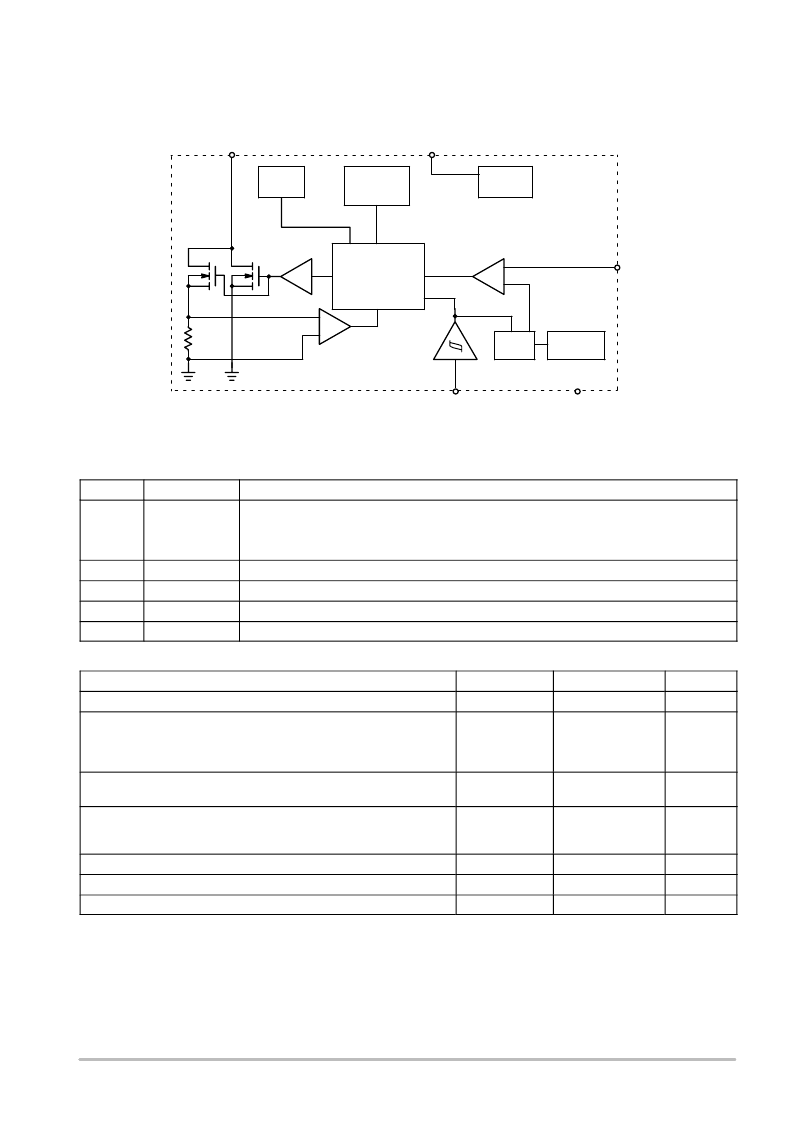
Figure 4. Representative Block Diagram
LX
PFM ON/OFF
Timing
Control
Driver
+
TSD
FB Fault
Protection
VDD
UVLO
+
Vref
SoftStart
PFM
Comparator
CE
GND
FB
PIN FUNCTION DESCRIPTION
Pin
Symbol
Description
1
CE
Chip Enable Pin
(1) The chip is enabled if a voltage which is equal to or greater than 0.9 V is applied.
(2) The chip is disabled if a voltage which is less than 0.3 V is applied.
(3) The chip will be enabled if it is left floating.
2
FB
PFM comparator inverting input, and is connected to offchip resistor divider which sets output voltage.
3
VDD
Power supply pin for internal circuit.
4
GND
Ground pin.
5
LX
External inductor connection pin.
MAXIMUM RATINGS
Rating
Symbol
Value
Unit
Power Supply Voltage (Pin 3)
VDD
0.3 to 6.0
V
Input/Output Pin
LX (Pin 5)
LX Peak Sink Current
FB (Pin 2)
V
LX
I
LX
V
FB
0.3 to 27
1.5
0.3 to 6.0
V
A
V
CE (Pin 1)
Input Voltage Range
V
CE
0.3 to 6.0
V
Power Dissipation and Thermal Characteristics
Maximum Power Dissipation @ T
A
= 25 C
Thermal Resistance, JunctiontoAir
P
D
R
JA
500
250
mW
C/W
Operating Ambient Temperature Range
T
A
40 to +85
C
Operating Junction Temperature Range
T
J
40 to +150
C
Storage Temperature Range
T
stg
55 to +150
C
Maximum ratings are those values beyond which device damage can occur. Maximum ratings applied to the device are individual stress limit values
(not normal operating conditions) and are not valid simultaneously. If these limits are exceeded, device functional operation is not implied, damage
may occur and reliability may be affected.
1. This device series contains ESD protection and exceeds the following tests:
Human Body Model (HBM)
2.0 kV per JEDEC standard: JESD22A114 for all pins.
Machine Model (MM)
200 V per JEDEC standard: JESD22A115 for all pins.
2. Latchup Current Maximum Rating:
150 mA per JEDEC standard: JESD78.
3. Moisture Sensitivity Level (MSL): 1 per IPC/JEDEC standard: JSTD020A.
相關(guān)PDF資料 |
PDF描述 |
|---|---|
| NCP1410DMR2 | 250 mA Sync-Rect PFM Step-Up DC-DC Converter with Low-Battery Detector |
| NCP1410 | 250 mA Sync-Rect PFM Step-Up DC-DC Converter with Low-Battery Detector |
| NCP1411DMR2 | Sync-Rect PFM Step-Up DC-DC Converter with Low-Battery Detector and Ring-Killer |
| NCP1411D | Sync-Rect PFM Step-Up DC-DC Converter with Low-Battery Detector and Ring-Killer |
| NCP1411DMR2G | Sync-Rect PFM Step-Up DC-DC Converter with Low-Battery Detector and Ring-Killer |
相關(guān)代理商/技術(shù)參數(shù) |
參數(shù)描述 |
|---|---|
| NCP1406V15GEVB | 功能描述:電源管理IC開(kāi)發(fā)工具 NCP1406 EVAL BRD RoHS:否 制造商:Maxim Integrated 產(chǎn)品:Evaluation Kits 類(lèi)型:Battery Management 工具用于評(píng)估:MAX17710GB 輸入電壓: 輸出電壓:1.8 V |
| NCP1406V25GEVB | 功能描述:電源管理IC開(kāi)發(fā)工具 NCP1406 EVAL BRD RoHS:否 制造商:Maxim Integrated 產(chǎn)品:Evaluation Kits 類(lèi)型:Battery Management 工具用于評(píng)估:MAX17710GB 輸入電壓: 輸出電壓:1.8 V |
| NCP1410DMR2 | 功能描述:直流/直流開(kāi)關(guān)轉(zhuǎn)換器 ANA DC-DC CONVERTER RoHS:否 制造商:STMicroelectronics 最大輸入電壓:4.5 V 開(kāi)關(guān)頻率:1.5 MHz 輸出電壓:4.6 V 輸出電流:250 mA 輸出端數(shù)量:2 最大工作溫度:+ 85 C 安裝風(fēng)格:SMD/SMT |
| NCP1410DMR2G | 功能描述:直流/直流開(kāi)關(guān)轉(zhuǎn)換器 ANA DC-DC CONVERTER RoHS:否 制造商:STMicroelectronics 最大輸入電壓:4.5 V 開(kāi)關(guān)頻率:1.5 MHz 輸出電壓:4.6 V 輸出電流:250 mA 輸出端數(shù)量:2 最大工作溫度:+ 85 C 安裝風(fēng)格:SMD/SMT |
| NCP1410GEVB | 功能描述:電源管理IC開(kāi)發(fā)工具 NCP1410 EVAL BRD RoHS:否 制造商:Maxim Integrated 產(chǎn)品:Evaluation Kits 類(lèi)型:Battery Management 工具用于評(píng)估:MAX17710GB 輸入電壓: 輸出電壓:1.8 V |
發(fā)布緊急采購(gòu),3分鐘左右您將得到回復(fù)。