- 您現在的位置:買賣IC網 > Datasheet目錄45 > NCP1601BDR2G (ON Semiconductor)IC PFC CTRL CRM/TRANSITION 8SOIC Datasheet資料下載
參數資料
| 型號: | NCP1601BDR2G |
| 廠商: | ON Semiconductor |
| 文件頁數: | 3/19頁 |
| 文件大小: | 257K |
| 描述: | IC PFC CTRL CRM/TRANSITION 8SOIC |
| 產品變化通告: | NCP1601BDR2G Discontinuation 11/May/2012 |
| 標準包裝: | 1 |
| 模式: | 臨界傳導(CRM),間歇式(轉換) |
| 頻率 - 開關: | 58kHz |
| 電流 - 啟動: | 17µA |
| 電源電壓: | 9.6 V ~ 18 V |
| 工作溫度: | -40°C ~ 125°C |
| 安裝類型: | 表面貼裝 |
| 封裝/外殼: | 8-SOIC(0.154",3.90mm 寬) |
| 供應商設備封裝: | 8-SOICN |
| 包裝: | 剪切帶 (CT) |
| 其它名稱: | NCP1601BDR2GOSCT |
NCP1601A, NCP1601B
http://onsemi.com
3
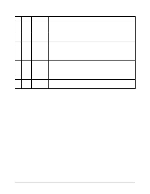
PIN FUNCTION DESCRIPTION
Pin
Symbol
Function
Function
1
FB
Feedback /
Shutdown
This pin receives a current I
FB
which is proportional to the PFC circuit output voltage. The current is
for the output regulation, output Overvoltage Protection (OVP), and output undervoltage protection
(UVP).
When I
FB
goes above 107% I
ref
, OVP is activated and the Drive Output is disabled.
When I
FB
goes below 8% I
ref
, the device enters a low- -current consumption shutdown mode.
2
V
control
Control
The voltage of this pin V
control
directly controls the input impedance and hence the power factor of
the circuit. This pin is connected to an external capacitor to limit the control voltage V
control
band-
width typically below 20 Hz to achieve Power Factor Correction.
3
Ramp
Ramp
This pin is connected to an external capacitor to set a ramp signal. The capacitor value directly
affects the input impedance of the PFC circuit and hence the maximum input power.
4
CS
Current Sense
This pin sources a current I
S
which depends on the inductor current and an offset voltage. The
current is for Overcurrent Protection (OCP) and zero current detection.
When I
S
is above 200 mA, OCP is activated and the Drive Output is disabled.
When I
S
is below 14 mA, the circuit detects a zero current. This information is used by the on- -time
modulation arrangement and by the oscillator block.
5
Osc
Oscillator /
Synchronization
In oscillator mode, this pin is connected to an external capacitor to set the oscillator frequency of
the DCM operation.
In synchronization mode, this pin is connected to an external driving signal. The positive edge of the
drive output is synchronized to the negative edge of the external signal in DCM operation.
If the inductor current is non- -zero at the end of a switching period, the output drive is not allowed to
turn on. CCM operation is prohibited. Instead, the circuit operates in CRM in this case.
6
GND
The IC ground
- -
7
Drv
Drive Output
This pin provides an output to an external MOSFET.
8
V
CC
Supply Voltage
This pin is the positive supply of the device. The operating range is between 9 V and 18 V with
UVLO start threshold 13.75 V for NCP1601A and 10.5 V for NCP1601B.
相關PDF資料 |
PDF描述 |
|---|---|
| NCP1603D100R2G | IC CTLR PFC/PWM COMBO 16-SOIC |
| NCP1605DR2G | IC PFC CONTROLLER CCM/DCM 16SOIC |
| NCP1606BDR2G | IC POWER FACTOR CONTROLLER 8SOIC |
| NCP1607BDR2G | IC PFC CONTROLLER CRM 8SOIC |
| NCP1611BDR2G | IC PFC CTLR HE ENHANCED 8-SOIC |
相關代理商/技術參數 |
參數描述 |
|---|---|
| NCP1601BP | 功能描述:功率因數校正 IC Fixed Frequency RoHS:否 制造商:Fairchild Semiconductor 開關頻率:300 KHz 最大功率耗散: 最大工作溫度:+ 125 C 安裝風格:SMD/SMT 封裝 / 箱體:SOIC-8 封裝:Reel |
| NCP1601BPG | 功能描述:功率因數校正 IC Fixed Frequency DCM/CRM PFC RoHS:否 制造商:Fairchild Semiconductor 開關頻率:300 KHz 最大功率耗散: 最大工作溫度:+ 125 C 安裝風格:SMD/SMT 封裝 / 箱體:SOIC-8 封裝:Reel |
| NCP1603D100R2 | 功能描述:功率因數校正 IC High Voltage Startup RoHS:否 制造商:Fairchild Semiconductor 開關頻率:300 KHz 最大功率耗散: 最大工作溫度:+ 125 C 安裝風格:SMD/SMT 封裝 / 箱體:SOIC-8 封裝:Reel |
| NCP1603D100R2G | 功能描述:功率因數校正 IC ANA PFC/PWM COMBO CONTROL RoHS:否 制造商:Fairchild Semiconductor 開關頻率:300 KHz 最大功率耗散: 最大工作溫度:+ 125 C 安裝風格:SMD/SMT 封裝 / 箱體:SOIC-8 封裝:Reel |
| NCP1605ADR2G | 功能描述:功率因數校正 IC ENHANCED PFC CNTRLER RoHS:否 制造商:Fairchild Semiconductor 開關頻率:300 KHz 最大功率耗散: 最大工作溫度:+ 125 C 安裝風格:SMD/SMT 封裝 / 箱體:SOIC-8 封裝:Reel |
發布緊急采購,3分鐘左右您將得到回復。