- 您現在的位置:買賣IC網 > Datasheet目錄45 > NCP1654BD133R2G (ON Semiconductor)IC PFC CCM 133KHZ 8-SOIC Datasheet資料下載
參數資料
| 型號: | NCP1654BD133R2G |
| 廠商: | ON Semiconductor |
| 文件頁數: | 14/23頁 |
| 文件大小: | 228K |
| 描述: | IC PFC CCM 133KHZ 8-SOIC |
| 標準包裝: | 2,500 |
| 模式: | 連續導電(CCM) |
| 頻率 - 開關: | 120kHz ~ 146kHz |
| 電流 - 啟動: | 75µA |
| 電源電壓: | 9 V ~ 20 V |
| 工作溫度: | -40°C ~ 125°C |
| 安裝類型: | 表面貼裝 |
| 封裝/外殼: | 8-SOIC(0.154",3.90mm 寬) |
| 供應商設備封裝: | 8-SOICN |
| 包裝: | 帶卷 (TR) |
| 其它名稱: | NCP1654BD133R2G-ND NCP1654BD133R2GOSTR |
NCP1654
http://onsemi.com
14
V
ramp
is the internal ramp voltage, the positive input of the
PFC modulation comparator,
V
m
is the multiplier voltage appearing on V
m
pin,
I
ch
is the internal charging current,
C
ramp
is the internal ramp capacitor, and
V
REF
is the internal reference voltage, the negative input of
the PFC modulation comparator.
I
ch
, C
ramp
, and V
REF
also act as the ramp signal of
switching frequency. Hence the charging current I
ch
is
specially designed as in (Equation 5). The multiplier
voltage V
m
is therefore expressed in terms of t
1
in
(Equation 6).
(eq. 5)
I
ch
+
C
ramp
V
REF
T
(eq. 6)
V
m
+ V
REF
*
t
1
C
ram
C
ramp
V
REF
T
+ V
REF
T * t
1
T
From (Equation 3) and (Equation 6), the input impedance
Z
in
is reformulated in (Equation 7).
(eq. 7)
Z
in
+
V
m
V
REF
V
out
I
L*50
Because V
REF
and V
out
are roughly constant versus time,
the multiplier voltage V
m
is designed to be proportional to
the I
L50
in order to have a constant Z
in
for PFC purpose.
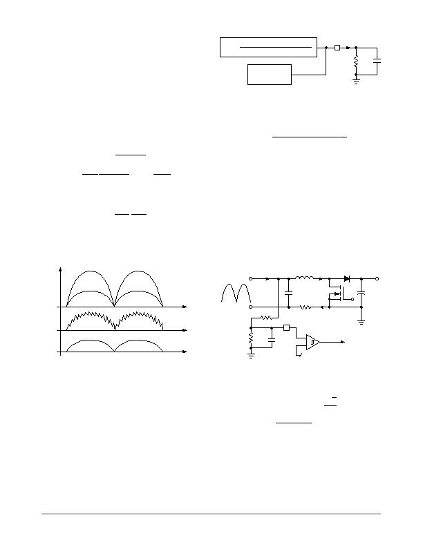
It is illustrated in Figure 34.
Figure 34. Multiplier Voltage Timing Diagram
Time
Time
Time
V
M
I
L
I
in
V
in
It can be seen in the timing diagram in Figure 33 that V
m
originally consists of a switching frequency ripple coming
from the inductor current I
L
. The duty ratio can be
inaccurately generated due to this ripple. This modulation
is the socalled
peak current mode
. Hence, an external
capacitor C
M
connected to the multiplier voltage V
m
pin is
essential to bypass the highfrequency component of V
m
.
The modulation becomes the socalled
average current
mode
with a better accuracy for PFC.
Figure 35. External Connection on the Multiplier
Voltage Pin
PFC Duty
Modulation
V
m
+
R
M
I
cs
V
bo
4(V
control
* V
CONTROL(min)
)
R
M
C
M
V
m
I
m
2
The multiplier voltage V
m
is generated according to
(Equation 8).
(eq. 8)
V
m
+
R
M
I
cs
V
bo
4(V
control
* V
CONTROL(min)
)
Where,
R
M
is the external multiplier resistor connected to V
m
pin,
which is constant.
V
bo
is the input voltage signal appearing on the BO pin,
which is proportional to the rms input voltage,
I
cs
is the sense current proportional to the inductor current
I
L
as described in (Equation 11).
V
control
is the control voltage signal, the output voltage of
Operational Transconductance Amplifier (OTA), as
described in (Equation 12).
R
M
directly limits the maximum input power capability
and hence its value affects the NCP1654 to operate in either
follower boost mode
or
constant output voltage mode
.
Figure 36. External Connection on the Brown Out Pin
Vbo
BO
4
+
R
boL
V
in
R
boU
C
BO
+
-
V
boH
/ V
boL
V
boH
= 1.3 V, V
boL
= 0.7 V
Refer to Figure 36,
(eq. 9)
V
bo
+ K
BO
(V
in
) + K
BO
@
2 2
p
V
ac
(eq. 10)
K
BO
+
R
boL
R
boU
) R
boL
where
V
bo
is the voltage on BO pin.
K
BO
is the decay ratio of V
in
to V
bo
.
<V
in
> is the average voltage signal of V
in
, the voltage
appearing on C
filter
.
V
ac
is the RMS input voltage.
相關PDF資料 |
PDF描述 |
|---|---|
| NCP1927DR2G | IC CTLR PFC/FLYBACK 16-SOIC |
| NCP380HMU21AATBG | IC CURRENT LIMIT SWITCH 6-UDFN |
| NCT1008DMT3R2G | TMP DIO MON/SMBUS 4CH 8WDFN |
| NCT210RQR2G | IC TEMP SENSOR LOC/REM 16QSOP |
| NCT214MT3R2G | IC TEMP SENSOR LOC/REM 10WDFN |
相關代理商/技術參數 |
參數描述 |
|---|---|
| NCP1654BD200R2G | 功能描述:功率因數校正 IC NCP1654 - 200KHZ RoHS:否 制造商:Fairchild Semiconductor 開關頻率:300 KHz 最大功率耗散: 最大工作溫度:+ 125 C 安裝風格:SMD/SMT 封裝 / 箱體:SOIC-8 封裝:Reel |
| NCP1654BD65R2G | 功能描述:功率因數校正 IC NCP1654-65K-B-SOIC RoHS:否 制造商:Fairchild Semiconductor 開關頻率:300 KHz 最大功率耗散: 最大工作溫度:+ 125 C 安裝風格:SMD/SMT 封裝 / 箱體:SOIC-8 封裝:Reel |
| NCP1654BP65G | 功能描述:功率因數校正 IC NCP1654-65K-B-PDIP RoHS:否 制造商:Fairchild Semiconductor 開關頻率:300 KHz 最大功率耗散: 最大工作溫度:+ 125 C 安裝風格:SMD/SMT 封裝 / 箱體:SOIC-8 封裝:Reel |
| NCP1654PFCGEVB | 功能描述:電源管理IC開發工具 NCP1654 PWR FACT CONT EVB RoHS:否 制造商:Maxim Integrated 產品:Evaluation Kits 類型:Battery Management 工具用于評估:MAX17710GB 輸入電壓: 輸出電壓:1.8 V |
| NCP1729-SKT | 制造商:P&S 功能描述:Sample Kit, including Two NCP1729SN35T1 and A Development Source CD-ROM 制造商:P&S 功能描述:Sample Kit,including Two NCP1729SN35T1 and A Development Source CD-ROM |
發布緊急采購,3分鐘左右您將得到回復。