- 您現在的位置:買賣IC網 > PDF目錄361111 > NE33200M (NEC Corp.) SUPER LOW NOISE HJ FET PDF資料下載
參數資料
| 型號: | NE33200M |
| 廠商: | NEC Corp. |
| 英文描述: | SUPER LOW NOISE HJ FET |
| 中文描述: | 超低噪聲黃建忠場效應管 |
| 文件頁數: | 1/7頁 |
| 文件大小: | 85K |
| 代理商: | NE33200M |
SUPER LOW NOISE HJ FET
NE33200
PART NUMBER
PACKAGE OUTLINE
NE33200
00 (Chip)
SYMBOLS
NF
OPT
1
PARAMETERS AND CONDITIONS
UNITS
MIN
TYP
MAX
Noise Figure, V
DS
= 2 V, I
D
= 10 mA,
f = 4 GHz
f = 12 GHz
Associated Gain, V
DS
= 2 V, I
D
= 10 mA,
f = 4 GHz
f = 12 GHz
Output Power at 1 dB Gain Compression Point, f = 12 GHz
V
DS
= 2 V, I
DS
= 10 mA
V
DS
= 2 V, I
DS
= 20 mA
Gain at P
1dB
, f = 12 GHz
V
DS
= 2 V, I
DS
= 10 mA
V
DS
= 2 V, I
DS
= 20 mA
Saturated Drain Current, V
DS
= 2 V, V
GS
= 0 V
Pinch-off Voltage, V
DS
= 2 V, I
D
= 100
μ
A
Transconductance, V
DS
= 2 V, I
D
= 10 mA
Gate to Source Leakage Current, V
GS
= -5 V
Thermal Resistance (Channel to Case)
dB
dB
0.35
0.75
1.0
G
A
1
dB
dB
15.0
10.5
9.5
P
1dB
dBm
dBm
11.2
12.0
G
1dB
dB
dB
mA
V
mS
μ
A
°
C/W
11.8
12.8
40
-0.8
70
0.5
I
DSS
V
P
g
m
I
GSO
15
-2.0
45
80
-0.2
10
240
R
TH(CH-C)2
Notes:
1. RF performance is determined by packaging and testing 10 samples per wafer. Wafer rejection criteria for standard devices is 2 rejects for
10 samples.
2. Chip mounted on infinite heat sink.
DESCRIPTION
The NE33200 is a Hetero-Junction FET chip that utilizes the
junction between Si-doped AlGaAs and undoped InGaAs to
create a two-dimensional electron gas layer with very high
electron mobility. Its excellent low noise figure and high
associated gain make it suitable for commercial and industrial
applications.
NEC's stringent quality assurance and test procedures as-
sure the highest reliability and performance.
FEATURES
VERY LOW NOISE FIGURE:
0.75 dB typical at 12 GHz
HIGH ASSOCIATED GAIN:
10.5 dB Typical at 12 GHz
GATE LENGTH:
0.3
μ
m
GATE WIDTH:
280
μ
m
ELECTRICAL CHARACTERISTICS
(T
A
= 25
°
C)
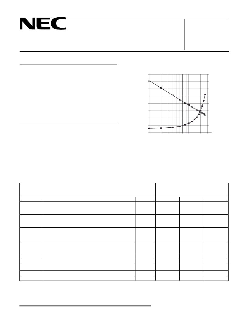
Frequency, f (GHz)
O
O
(
A
A
NOISE FIGURE & ASSOCIATED
GAIN vs. FREQUENCY
V
DS
= 2 V, I
DS
= 10 mA
California Eastern Laboratories
4
3.5
3
2.5
2
1.5
1
0.5
0
Ga
NF
1 10 30
24
21
18
15
12
9
6
3
0
相關PDF資料 |
PDF描述 |
|---|---|
| NE33200N | SUPER LOW NOISE HJ FET |
| NE33284A-T1 | KJ 6C 6#12 PIN PLUG |
| NE33284A-T1A | L to X BAND SUPER LOW NOISE AMPLIFIER N-CHANNEL HJ-FET |
| NE33284 | L to X BAND SUPER LOW NOISE AMPLIFIER N-CHANNEL HJ-FET |
| NE33284A | L to X BAND SUPER LOW NOISE AMPLIFIER N-CHANNEL HJ-FET |
相關代理商/技術參數 |
參數描述 |
|---|---|
| NE33200N | 制造商:NEC 制造商全稱:NEC 功能描述:SUPER LOW NOISE HJ FET |
| NE33284 | 制造商:NEC 制造商全稱:NEC 功能描述:L to X BAND SUPER LOW NOISE AMPLIFIER N-CHANNEL HJ-FET |
| NE33284A | 制造商:NEC 制造商全稱:NEC 功能描述:L to X BAND SUPER LOW NOISE AMPLIFIER N-CHANNEL HJ-FET |
| NE33284A_98 | 制造商:NEC 制造商全稱:NEC 功能描述:SUPER LOW NOISE HJ FET |
| NE33284AS | 制造商:NEC 制造商全稱:NEC 功能描述:SUPER LOW NOISE HJ FET |
發布緊急采購,3分鐘左右您將得到回復。