- 您現在的位置:買賣IC網 > PDF目錄382378 > PCA8515 (NXP Semiconductors N.V.) Stand-alone OSD PDF資料下載
參數資料
| 型號: | PCA8515 |
| 廠商: | NXP Semiconductors N.V. |
| 英文描述: | Stand-alone OSD |
| 中文描述: | 單機OSD |
| 文件頁數: | 19/64頁 |
| 文件大小: | 405K |
| 代理商: | PCA8515 |
第1頁第2頁第3頁第4頁第5頁第6頁第7頁第8頁第9頁第10頁第11頁第12頁第13頁第14頁第15頁第16頁第17頁第18頁當前第19頁第20頁第21頁第22頁第23頁第24頁第25頁第26頁第27頁第28頁第29頁第30頁第31頁第32頁第33頁第34頁第35頁第36頁第37頁第38頁第39頁第40頁第41頁第42頁第43頁第44頁第45頁第46頁第47頁第48頁第49頁第50頁第51頁第52頁第53頁第54頁第55頁第56頁第57頁第58頁第59頁第60頁第61頁第62頁第63頁第64頁
1995 Jan 19
19
Philips Semiconductors
Preliminary specification
Stand-alone OSD
PCA8515
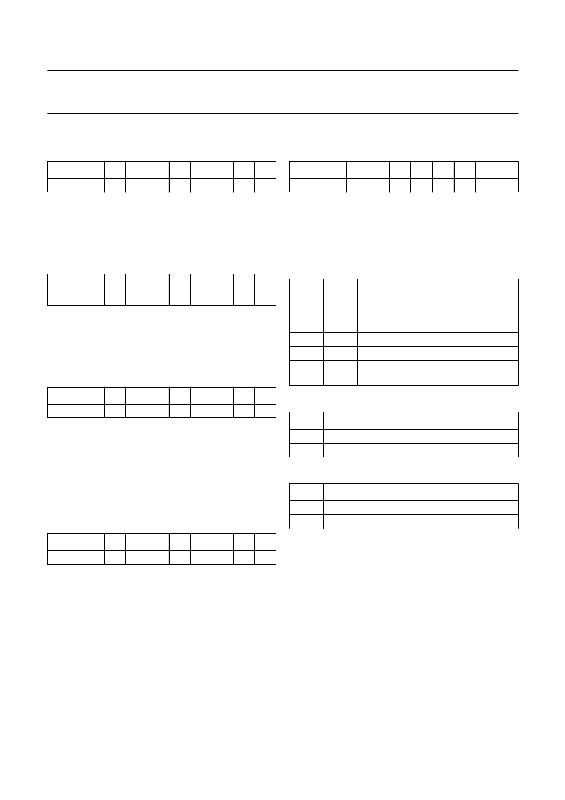
9.4
Command 3
Table 19
Command 3 format
Command 3 loads the DCR Address Register with the
4 MSBs of the RAM address to which data will be written.
9.5
Command 4
Table 20
Command 4 format
Command 4 loads the DCR Address Register with the
4 LSBs of the RAM address to which data will be written.
9.6
Command 5
Table 21
Command 5 format
Command 5 is used to load character data into the DCR
Character Register. The data will specify either a
Character Font Code, the Test Code, the Carriage Return
Code or the Space Code. These codes are explained in
detail in Section 8.1.
9.7
Command 6
Table 22
Command 6 format
Command 6 loads the programmable 6-bit counter of the
OSD clock oscillator. The output frequency (f
OSD
) is a
function of the decimal value of the 6-bits loaded in by
Command 6. See Chapter 11.
BS1
BS0
7
6
5
4
3
2
1
0
0
0
0
0
1
1
A7
A6
A5
A4
BS1
BS0
7
6
5
4
3
2
1
0
0
0
0
0
1
1
A3
A2
A1
A0
BS1
BS0
7
6
5
4
3
2
1
0
1
0
1
C6
C5
C4
C3
C2
C1
C0
BS1
BS0
7
6
5
4
3
2
1
0
0
1
0
0
D5
D4
D3
D2
D1
D0
9.8
Command 7
Table 23
Command 7 format
This command loads Control Register 1 with data that
selects the scan mode, the output polarity of signals FB,
ACM, R, G, B and I, and also enables/disables the OSD
clock.
Table 24
Selection of Scan Mode
Table 25
Selection of output polarity (see Fig.13)
Table 26
OSD clock control
BS1
BS0
7
6
5
4
3
2
1
0
0
1
0
1
0
0
M1
M0
Bp
EN
M1
M0
SCAN MODE
0
0
NTSC - 525LPF/60 Hz or
PAL 625LPF/50 Hz; see Fig.11. This is
the default setting.
reserved
reserved
PAL 1250LPF/100 Hz - PAL; see
Fig.12.
0
1
1
1
0
1
Bp
OUTPUT POLARITY (FB, ACM, R, G, B, I)
0
1
active LOW
active HIGH (the default setting)
EN
OSD CLOCK
0
1
disabled (the default setting)
enabled
相關PDF資料 |
PDF描述 |
|---|---|
| PCA8515P | Stand-alone OSD |
| PCA8515T | Stand-alone OSD |
| PCA8516T | Stand-alone OSD |
| PCA8516 | Stand-alone OSD |
| PCA8516P | Stand-alone OSD |
相關代理商/技術參數 |
參數描述 |
|---|---|
| PCA8515P | 制造商:PHILIPS 制造商全稱:NXP Semiconductors 功能描述:Stand-alone OSD |
| PCA8515T | 制造商:PHILIPS 制造商全稱:NXP Semiconductors 功能描述:Stand-alone OSD |
| PCA8515T/009 | 制造商:NXP Semiconductors 功能描述:ON-SCREEN DISPLAY IC, PDSO24 |
| PCA8516 | 制造商:PHILIPS 制造商全稱:NXP Semiconductors 功能描述:Stand-alone OSD |
| PCA85162 | 制造商:PHILIPS 制造商全稱:NXP Semiconductors 功能描述:Universal LCD driver for low multiplex rates |
發布緊急采購,3分鐘左右您將得到回復。