- 您現在的位置:買賣IC網 > PDF目錄382383 > PCM1717 Stereo Audio DIGITAL-TO-ANALOG CONVERTER PDF資料下載
參數資料
| 型號: | PCM1717 |
| 英文描述: | Stereo Audio DIGITAL-TO-ANALOG CONVERTER |
| 中文描述: | 立體聲音頻數字模擬轉換器 |
| 文件頁數: | 3/14頁 |
| 文件大小: | 126K |
| 代理商: | PCM1717 |
3
PCM1717
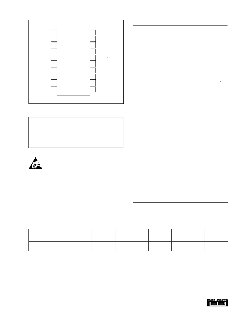
PIN ASSIGNMENTS
XTI
DGND
V
DD
LRCIN
DIN
BCKIN
ZERO
D/C_R
V
OUT
R
AGND
XTO
CLKO
ML/MUTE
MC/DM1
MD/DM0
RSTB
MODE
DC_L
V
OUT
L
V
CC
1
2
3
4
5
6
7
8
9
10
20
19
18
17
16
15
14
13
12
11
PIN CONFIGURATION
PIN
NAME
FUNCTION
Data Input Interface Pins
4
5
LRCIN
DIN
Sample Rate Clock Input. Controls the update rate (fs).
Serial Data Input. MSB first, right justified (Sony format)
or I
2
S (Philips). Contains a frame of 16- or 18-bit data.
Bit Clock Input. Clocks in the data present on DIN input.
6
BCKIN
Mode Control and Clock Signals
1
XTI
Oscillator Input (External Clock Input). For an internal
clock, tie XTI to one side of the crystal oscillator. For an
external clock, tie XTI to the output of the chosen
external clock.
Operation Mode Select. For Software Mode, tie Mode
“HIGH”. For Hardware Mode, tie Mode “LOW”.
Mode Control for Data Input or De-emphasis. When
“HIGH” MD is selected, and a “LOW” selects DM0.
Mode Control for BCKIN or De-emphasis. When “HIGH”,
MC is selected, and a “LOW” selects DM1.
Mode Control for Strobe Clock or Mute. When “HIGH”,
ML is selected, and a “LOW” selects mute.
Buffered Output of Oscillator. Equivalent to XTI.
Oscillator Output. When using the internal clock, tie to
the opposite side (from pin 1) of the crystal oscillator.
When using an external clock, leave XTO open.
14
MODE
16
MD/DM0
17
MC/DM1
18
ML/MUTE
19
20
CLKO
XTO
Operational Controls and Flags
7
ZERO
Infinite Zero Detection Flag, open drain output. When
the zero detection feature is muting the output, ZERO
is “LOW”. When non-zero input data is present, ZERO
is in a high impedance state. When the input data is
continuously zero for 65.536 BCKIN cycles, zero will be
low.
Resets DAC operation with an active “LOW” pulse.
15
RSTB
Analog Output Functions
8
D/C_R
Right Channel Output Amplifier Common. Bypass to
ground with 10
μ
F capacitor.
Right Channel Analog Output. V
OUT
max = 0.62 x V
CC
.
Left Channel Analog Output. V
OUT
max = 0.62 x V
CC
.
Left Channel Output Amplifier Common. Bypass to
ground with 10
μ
F capacitor.
9
12
13
V
OUT
R
V
OUT
L
D/C_L
Power Supply Connections
2
3
10
11
DGND
V
DD
AGND
V
CC
Digital Ground.
Digital Power Supply (+5V).
Analog Ground.
Analog Power Supply (+3V).
The information provided herein is believed to be reliable; however, BURR-BROWN assumes no responsibility for inaccuracies or omissions. BURR-BROWN assumes no
responsibility for the use of this information, and all use of such information shall be entirely at the user’s own risk. Prices and specifications are subject to change without notice.
No patent rights or licenses to any of the circuits described herein are implied or granted to any third party. BURR-BROWN does not authorize or warrant any BURR-BROWN
product for use in life support devices and/or systems.
Power Supply Voltage ...................................................................... +6.5V
+V
to +V
Difference ...................................................................
±
0.1V
Input Logic Voltage .................................................. –0.3V to (V
+ 0.3V)
Power Dissipation .......................................................................... 200mW
Operating Temperature Range ......................................... –25
°
C to +85
°
C
Storage Temperature ...................................................... –55
°
C to +125
°
C
Lead Temperature (soldering, 5s).................................................. +260
°
C
Thermal Resistance,
θ
JA.......................................................................................
+70
°
C/W
ABSOLUTE MAXIMUM RATINGS
ELECTROSTATIC
DISCHARGE SENSITIVITY
This integrated circuit can be damaged by ESD. Burr-Brown
recommends that all integrated circuits be handled with
appropriate precautions. Failure to observe proper handling
and installation procedures can cause damage.
ESD damage can range from subtle performance degradation
to complete device failure. Precision integrated circuits may
be more susceptible to damage because very small parametric
changes could cause the device not to meet its published
specifications.
PACKAGE
DRAWING
NUMBER
SPECIFIED
TEMPERATURE
RANGE
PACKAGE
MARKING
ORDERING
NUMBER
(1)
TRANSPORT
MEDIA
PRODUCT
PACKAGE
PCM1717E
SSOP-20
"
334-1
"
–25
°
C to +85
°
C
"
PCM1717E
"
PCM1717E
PCM1717E/2K
Rails
"
Tape and Reel
NOTE: (1) Models with a slash (/) are available only in Tape and Reel in the quantities indicated (e.g., /2K indicates 2000 devices per reel). Ordering 2000 pieces
of “PCM1717E/2K” will get a single 2000-piece Tape and Reel.
PACKAGE/ORDERING INFORMATION
相關PDF資料 |
PDF描述 |
|---|---|
| PCM1717E | Stereo Audio DIGITAL-TO-ANALOG CONVERTER |
| PCM1718 | Stereo Audio DIGITAL-TO-ANALOG CONVERTER |
| PCM1718E | Stereo Audio DIGITAL-TO-ANALOG CONVERTER |
| PCM1719 | Stereo Audio DIGITAL-TO-ANALOG CONVERTER |
| PCM1719E | Stereo Audio DIGITAL-TO-ANALOG CONVERTER |
相關代理商/技術參數 |
參數描述 |
|---|---|
| PCM1717E | 功能描述:音頻數/模轉換器 IC SoundPlus Stereo DAC RoHS:否 制造商:Texas Instruments 轉換器數量: 分辨率:16 bit 接口類型:I2S, UBS 轉換速率: 信噪比:98 dB 工作電源電壓:5 V DAC 輸出端數量:2 工作溫度范圍:- 25 C to + 85 C 電源電流:23 mA 安裝風格:SMD/SMT 封裝 / 箱體:TQFP-32 封裝:Reel |
| PCM1717E/2K | 功能描述:音頻數/模轉換器 IC SoundPlus Stereo DAC RoHS:否 制造商:Texas Instruments 轉換器數量: 分辨率:16 bit 接口類型:I2S, UBS 轉換速率: 信噪比:98 dB 工作電源電壓:5 V DAC 輸出端數量:2 工作溫度范圍:- 25 C to + 85 C 電源電流:23 mA 安裝風格:SMD/SMT 封裝 / 箱體:TQFP-32 封裝:Reel |
| PCM1717E/2KG4 | 功能描述:音頻數/模轉換器 IC SoundPlus Stereo DAC RoHS:否 制造商:Texas Instruments 轉換器數量: 分辨率:16 bit 接口類型:I2S, UBS 轉換速率: 信噪比:98 dB 工作電源電壓:5 V DAC 輸出端數量:2 工作溫度范圍:- 25 C to + 85 C 電源電流:23 mA 安裝風格:SMD/SMT 封裝 / 箱體:TQFP-32 封裝:Reel |
| PCM1717EG | 功能描述:音頻數/模轉換器 IC SoundPlus Stereo DAC RoHS:否 制造商:Texas Instruments 轉換器數量: 分辨率:16 bit 接口類型:I2S, UBS 轉換速率: 信噪比:98 dB 工作電源電壓:5 V DAC 輸出端數量:2 工作溫度范圍:- 25 C to + 85 C 電源電流:23 mA 安裝風格:SMD/SMT 封裝 / 箱體:TQFP-32 封裝:Reel |
發布緊急采購,3分鐘左右您將得到回復。