- 您現在的位置:買賣IC網 > PDF目錄382384 > PCM1850 24-BIT, 96-kHz STEREO A/D CONVERTER WITH 6 X 2-CHANNEL MUX AND PGA PDF資料下載
參數資料
| 型號: | PCM1850 |
| 英文描述: | 24-BIT, 96-kHz STEREO A/D CONVERTER WITH 6 X 2-CHANNEL MUX AND PGA |
| 中文描述: | 24位,96千赫立體聲A / D轉換器6 × 2通道的MUX和PGA |
| 文件頁數: | 22/30頁 |
| 文件大小: | 370K |
| 代理商: | PCM1850 |
第1頁第2頁第3頁第4頁第5頁第6頁第7頁第8頁第9頁第10頁第11頁第12頁第13頁第14頁第15頁第16頁第17頁第18頁第19頁第20頁第21頁當前第22頁第23頁第24頁第25頁第26頁第27頁第28頁第29頁第30頁
PCM1850
PCM1851
SLES108
MARCH 2004
www.ti.com
22
HPF Bypass Control
The built-in HPF function for dc component rejection can be bypassed via the serial port. In bypass mode, the dc component
of the analog input signal, the internal dc offset, etc., are converted and included in the digital output data.
BYP
HPF (HIGH-PASS FILTER) MODE
0
Normal (no dc component on DOUT) mode (default)
1
Bypass (dc component on DOUT) mode
System Reset Control
The system reset control is used to resynchronize the system via the serial port when the system clock frequency, interface
mode, and data format are changed. Change them while SRST = LOW. If they are changed during normal operation, analog
performance can be degraded.
SRST
SYSTEM RESET
0
Resynchronization
1
Normal operation (default)
Mode Register Reset Control
The MRST bit is used to reset the mode control register to its default settings via the serial port.
MRST
MODE REGISTER RESET
0
Set default value
1
Normal operation (default)
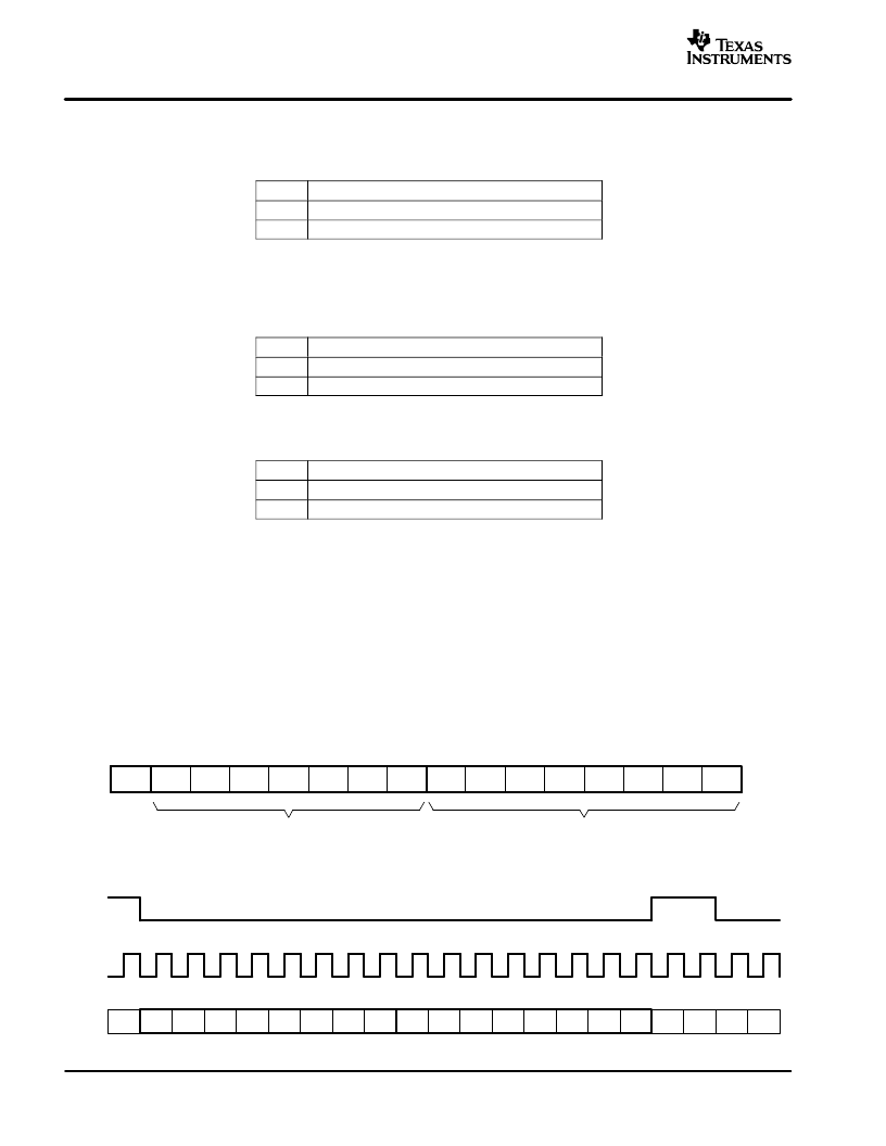
SPI SERIAL CONTROL PORT FOR MODE CONTROL (PCM1850)
The user-programmable built-in functions of the PCM1850 can be controlled through a serial control port with the SPI
format. All operations for the serial control port use 16-bit data words. Figure 27 shows the control data word format. The
most significant bit must be set to 0. There are seven bits, labeled IDX[6:0], that set the register index (or address) for write
operations. The least significant eight bits, D[7:0], contain the data to be written to the register specified by IDX[6:0].
Figure 28 shows the functional timing diagram for writing to the serial control port. MS (pin 30) is held at a logic 1 state until
a register needs to be written. To start the register write cycle, MS is set to logic 0. Sixteen clocks are then provided on MC
(pin 31), corresponding to the 16 bits of the control data word on MD (pin 32). After the sixteenth clock cycle has completed,
the data is latched into the indexed mode control register in the write operation. To write the next data word, MS must be
set to 1 once.
MSB
LSB
Register Index (or Address)
Register Data
0
IDX6
IDX5
IDX4
IDX3
IDX2
IDX1
IDX0
D7
D6
D4
D5
D3
D2
D1
D0
Figure 27. Control Data Word Format for MD
IDX0
D7
D6
D4
D5
D3
D2
D1
D0
MS
MC
MD
IDX1
IDX2
IDX3
IDX4
IDX5
IDX6
0
X
X
X
0
IDX6
Figure 28. Serial Control Format
相關PDF資料 |
PDF描述 |
|---|---|
| PCM1851 | 24-BIT, 96-kHz STEREO A/D CONVERTER WITH 6 X 2-CHANNEL MUX AND PGA |
| PCM1851PJT | 24-BIT, 96-kHz STEREO A/D CONVERTER WITH 6 X 2-CHANNEL MUX AND PGA |
| PCM2702 | 16-Bit Stereo DIGITAL-TO-ANALOG CONVERTER with Interface |
| PCM2702E | 16-Bit Stereo DIGITAL-TO-ANALOG CONVERTER with Interface |
| PCM3000 | Stereo Audio CODEC 18-BITS, SERIAL INTERFACE TM |
相關代理商/技術參數 |
參數描述 |
|---|---|
| PCM-1850-06 | 制造商:Distributed By MCM 功能描述:6 ft DB9 Serial Cable Female to Female |
| PCM-1850-10 | 制造商:Distributed By MCM 功能描述:10 ft DB9 Serial Cable Female to Female |
| PCM1850APJT | 功能描述:音頻模/數轉換器 IC 24-Bit Audio ADC RoHS:否 制造商:Wolfson Microelectronics 轉換速率: 分辨率: ADC 輸入端數量: 工作電源電壓: 最大工作溫度: 最小工作溫度: 安裝風格: 封裝 / 箱體: 封裝: |
| PCM1850APJTG4 | 功能描述:音頻模/數轉換器 IC 24B Stereo Audio ADC RoHS:否 制造商:Wolfson Microelectronics 轉換速率: 分辨率: ADC 輸入端數量: 工作電源電壓: 最大工作溫度: 最小工作溫度: 安裝風格: 封裝 / 箱體: 封裝: |
| PCM1850APJTR | 功能描述:音頻模/數轉換器 IC 24-Bit Audio ADC RoHS:否 制造商:Wolfson Microelectronics 轉換速率: 分辨率: ADC 輸入端數量: 工作電源電壓: 最大工作溫度: 最小工作溫度: 安裝風格: 封裝 / 箱體: 封裝: |
發布緊急采購,3分鐘左右您將得到回復。