- 您現在的位置:買賣IC網 > PDF目錄382390 > PGA309 Voltage Output PROGRAMMABLE SENSOR CONDITIONER PDF資料下載
參數資料
| 型號: | PGA309 |
| 英文描述: | Voltage Output PROGRAMMABLE SENSOR CONDITIONER |
| 中文描述: | 電壓輸出可編程傳感器空調 |
| 文件頁數: | 7/20頁 |
| 文件大小: | 298K |
| 代理商: | PGA309 |
"#$%
SBOS292A DECEMBER 2003 REVISED AUGUST 2004
www.ti.com
7
ELECTRICAL CHARACTERISTICS (continued)
BOLDFACE
limits apply over the specified temperature range:
T
A
= 40
°
C to +125
°
C
TA = +25
°
C, VSA = VSD = +5V (VSA = VSUPPLY ANALOG, VSD = VSUPPLY DIGITAL; VSA must equal VSD), GNDD = GNDA = 0, and VREF = REFIN/REFOUT = +5V,
unless otherwise noted.
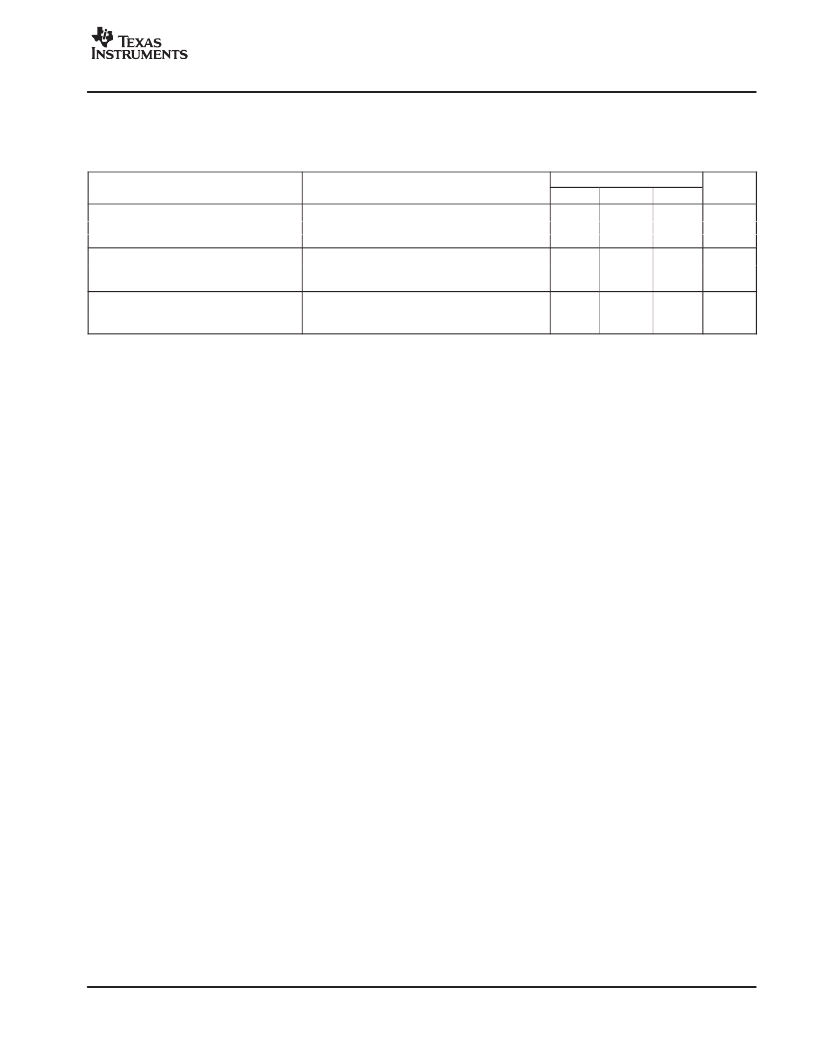
PGA309
PARAMETER
UNITS
MAX
TYP
MIN
CONDITIONS
POWER SUPPLY
VSA, VSD
ISA + ISD, Quiescent Current
POWER-ON RESET
Power-Up Threshold
Power-Down Threshold
2.7
5.5
1.6
V
VSA = VSD = +5V, without Bridge Load
1.2
mA
VSA Rising
VSA Falling
2.2
1.7
2.7
V
V
TEMPERATURE RANGE
Specified Performance
Operational Degraded Performance
40
55
+125
+150
°
C
°
C
(1)PGA309 total differential gain from input (VIN1VIN2) to output (VOUT). VOUT / (VIN1VIN2) = (Front-End PGA gain) (Output Amplifier gain) (Gain DAC).
(2)RTI = referred to input. RTO = referred to output.
(3)Linear input range is the allowed min/max voltage on the VIN1 and VIN2 pins for the input PGA to continue to operate in a linear region. The allowed
common-mode and differential voltage is dependent upon gain and offset settings. Refer to the Gain Scaling section for more information.
(4)Unless limited by over/under-scale setting.
(5)When VEXC is enabled, a minimum reference selector circuit becomes the reference for the comparator threshold. This minimum reference
selector circuit uses VEXC 100mV and VSA 1.2V and compares the VINX pin to the lower of the two references. This ensures accurate fault
monitoring in conditions where VEXC might be higher or lower than the input CMR of the PGA input amplifier relative to VSA.
(6)Lookup Table allows multislope compensation over temperature. Lookup Table has access to 17 calibration points consisting of 3 adjustment
values (Tx, Temperature, ZMx, Zero DAC, GMx, Gain DAC) that are stored in 16-bit data format (17x3x16 = Lookup Table size).
相關PDF資料 |
PDF描述 |
|---|---|
| PGA309AIPWR | Voltage Output PROGRAMMABLE SENSOR CONDITIONER |
| PGA309AIPWT | Voltage Output PROGRAMMABLE SENSOR CONDITIONER |
| PH1113-100 | Radar Pulsed Power Transistor - 100 Watts, 1.1-1.3 GHz, 3ms Pulse, 30% Duty |
| PH1214-8M | Radar Pulsed Power Transistor, SW, loops Pulse, 10% Duty 1.2 - 1.4 GHz |
| PH20100S | N-channel TrenchMOS standard level FET |
相關代理商/技術參數 |
參數描述 |
|---|---|
| PGA309_05 | 制造商:BB 制造商全稱:BB 功能描述:Voltage Output PROFRAMMABLE SENSOR CONDITIONER |
| PGA309_11 | 制造商:TI 制造商全稱:Texas Instruments 功能描述:Voltage Output Programmable Sensor Conditioner |
| PGA309AIPWR | 功能描述:電流靈敏放大器 PGA309 Voltage Out Prog Sensor Cndtner RoHS:否 制造商:Texas Instruments 通道數量: 共模抑制比(最小值):110 dB 輸入補償電壓:80 uV 電源電壓-最大:5.5 V 電源電壓-最小:2.7 V 電源電流:350 uA 最大工作溫度:+ 125 C 最小工作溫度:- 40 C 安裝風格:SMD/SMT 封裝 / 箱體:VQFN-16 封裝:Reel |
| PGA309AIPWRG4 | 功能描述:電流靈敏放大器 PGA309 Voltage Out Prog Sensor Cndtner RoHS:否 制造商:Texas Instruments 通道數量: 共模抑制比(最小值):110 dB 輸入補償電壓:80 uV 電源電壓-最大:5.5 V 電源電壓-最小:2.7 V 電源電流:350 uA 最大工作溫度:+ 125 C 最小工作溫度:- 40 C 安裝風格:SMD/SMT 封裝 / 箱體:VQFN-16 封裝:Reel |
| PGA309AIPWT | 功能描述:電流靈敏放大器 PGA309 Voltage Out Prog Sensor Cndtner RoHS:否 制造商:Texas Instruments 通道數量: 共模抑制比(最小值):110 dB 輸入補償電壓:80 uV 電源電壓-最大:5.5 V 電源電壓-最小:2.7 V 電源電流:350 uA 最大工作溫度:+ 125 C 最小工作溫度:- 40 C 安裝風格:SMD/SMT 封裝 / 箱體:VQFN-16 封裝:Reel |
發布緊急采購,3分鐘左右您將得到回復。