- 您現(xiàn)在的位置:買賣IC網(wǎng) > PDF目錄2108 > PI74SSTVF16859AE (Pericom)IC REG BUFFER 13-26BIT 64-TSSOP PDF資料下載
參數(shù)資料
| 型號: | PI74SSTVF16859AE |
| 廠商: | Pericom |
| 文件頁數(shù): | 1/8頁 |
| 文件大小: | 0K |
| 描述: | IC REG BUFFER 13-26BIT 64-TSSOP |
| 標(biāo)準(zhǔn)包裝: | 28 |
| 系列: | 74SSTVF |
| 邏輯類型: | 13 位至 26 位寄存緩沖器,DDR |
| 電源電壓: | 2.3 V ~ 2.7 V |
| 位數(shù): | 13,26 |
| 工作溫度: | 0°C ~ 70°C |
| 安裝類型: | 表面貼裝 |
| 封裝/外殼: | 64-TFSOP (0.240",6.10mm 寬) |
| 供應(yīng)商設(shè)備封裝: | 64-TSSOP |
| 包裝: | 管件 |
1
PS8657C
10/07/08
ProductDescription
PericomSemiconductor’sPI74SSTVF16859logiccircuitisproduced
using the Company’s advanced sub-micron CMOS technology,
achieving industry leading speed.
All inputs are compatible with the JEDEC standard for SSTL_2,
except the LVCMOS reset (RESET) input. All outputs are SSTL_2,
Class II compatible.
The device operates from a differential clock (CLK and CLK). Data
registeredatthecrossingofCLKgoingHIGH,andCLKgoingLOW.
ThePI74SSTVF16859supportslow-powerstandbyoperation.When
RESET is LOW, the differential input receivers are disabled, and
undriven (floating) data, clock and reference voltage (VREF) inputs
are allowed. In addition, when RESET is LOW, all registers are reset,
and all outputs are forced LOW. The LVCMOS RESET input must
always be held at a valid logic HIGH or LOW level.
To ensure defined outputs from the register before a stable clock
has been supplied, RESET must be held in the LOW state during
power up.
In the DDR DIMM application, RESET is specified to be completely
asynchronous with respect to CLK and CLK. Therefore, no timing
relationship can be guaranteed between the two. When entering
RESET, the register will be cleared and the outputs will be driven
LOW quickly, relative to the time to disable the differential input
receivers, thus ensuring no glitches on the output. However, when
comingoutof RESET,theregisterwillbecomeactivequickly,relative
to the time to enable the differential input receivers. When the data
inputs are LOW, and the clock is stable, during the time from the
LOW-to-HIGH transition of RESET until the input receivers
are fully enabled, the design must ensure that the outputs will
remainLOW.
Pericom’s PI74SSTVF16859 is characterized for operation from
0°Cto70°C.
ProductFeatures
PI74 SSTVF16859 is designed for low-voltage operation,
2.5VforPC1600~PC2700;2.6VforPC3200
Supports SSTL_2 Class I specifications on outputs
All Inputs are SSTL_2 Compatible, except RESET
whichisLVCMOS.
Designed for DDR Memory
Flow-Through Architecture
Packages:
56-pin, Plastic Very Thin Fine Pitch Quad Flat
No Lead QFN (ZB)
(Lead-free packages are available)
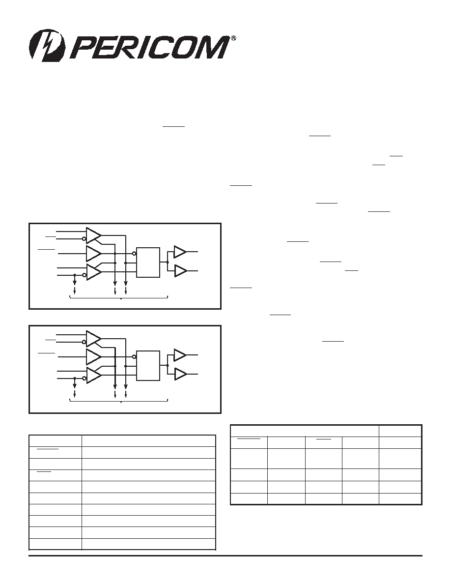
Logic Block Diagram - TSSOP
ProductPinDescription
12345678901234567890123456789012123456789012345678901234567890121234567890123456789012345678901212345678901234567890123456789012123456789012
PI74SSTVF16859
13-Bit to 26-Bit Registered Buffer
TO 12 OTHER CHANNELS
RESET
CLK
48
49
VREF
D1
35
45
D
R
CLK
Q1A
16
Q1B
32
CLK
V
51
Logic Block Diagram - QFN
TO 12 OTHER CHANNELS
RESET
CLK
35
36
VREF
D1
24
32
D
R
CLK
Q1A
7
Q1B
22
CLK
V
38
s
t
u
p
n
Is
t
u
p
t
u
O
T
E
S
E
RK
L
CK
L
CD
Q
L
r
o
X
g
n
it
a
o
l
F
r
o
X
g
n
it
a
o
l
F
r
o
X
g
n
it
a
o
l
F
L
H
↑↓
HH
Η↑
↓
LL
HH
r
o
LH
r
o
LX
o
Q
)
2
(
Truth
Table(1)
Notes:
1. H = High Signal Level
L = Low Signal Level
↑ = Transition LOW-to-HIGH
↓ = Transition HIGH-to-LOW
X = Irrelevant or floating
2. Output level before the
indicated steady state
input conditions were
established.
e
m
a
N
n
i
Pn
o
i
t
p
i
r
c
s
e
D
T
E
S
E
RS
O
M
C
V
L
)
w
o
L
e
v
it
c
A
(
t
e
s
e
R
K
L
Ct
u
p
n
I
l
a
it
n
e
r
e
f
fi
D
e
v
it
i
s
o
P
,t
u
p
n
I
k
c
o
l
C
K
L
Ct
u
p
n
I
l
a
it
n
e
r
e
f
fi
D
e
v
it
a
g
e
N
,t
u
p
n
I
k
c
o
l
C
D3
1
D
-
1
D
,t
u
p
n
I
a
t
a
D
Q3
1
Q
-
1
Q
,t
u
p
t
u
O
a
t
a
D
N
Gd
n
u
o
r
G
V D
D
e
g
a
tl
o
V
y
l
p
u
S
e
r
o
C
V Q
D
e
g
a
tl
o
V
y
l
p
u
S
t
u
p
t
u
O
V F
E
R
e
g
a
tl
o
V
e
c
n
e
r
e
f
e
R
t
u
p
n
I
08-0291
相關(guān)PDF資料 |
PDF描述 |
|---|---|
| PI74SSTVF16859AZBE | IC REG BUFFER 13-26BIT 56-QFN |
| PI74STX1G02CX | IC SINGLE 2-IN NOR GATE SC70-5 |
| PI74STX1GU04CEX | IC UNBUFFERED INVERTER SC70-5 |
| PI74STX4G4245ZJEX | IC 2BIT LVL SHFT BUF/TXRX 16TDFN |
| PI90LVB16L | IC CLOCK BUFFER MUX 1:6 24-TSSOP |
相關(guān)代理商/技術(shù)參數(shù) |
參數(shù)描述 |
|---|---|
| PI74SSTVF16859AEX | 功能描述:寄存器 13/26B Registered Buffer RoHS:否 制造商:NXP Semiconductors 邏輯類型:CMOS 邏輯系列:HC 電路數(shù)量:1 最大時鐘頻率:36 MHz 傳播延遲時間: 高電平輸出電流:- 7.8 mA 低電平輸出電流:7.8 mA 電源電壓-最大:6 V 最大工作溫度:+ 125 C 封裝 / 箱體:SOT-38 封裝:Tube |
| PI74SSTVF16859AX | 制造商:Pericom Semiconductor Corporation 功能描述:Registered Buffer Single 13-CH CMOS 64-Pin TSSOP T/R |
| PI74SSTVF16859AZBE | 功能描述:IC REG BUFFER 13-26BIT 56-QFN RoHS:是 類別:集成電路 (IC) >> 邏輯 - 專用邏輯 系列:74SSTVF 產(chǎn)品變化通告:Product Discontinuation 25/Apr/2012 標(biāo)準(zhǔn)包裝:1,500 系列:74SSTV 邏輯類型:DDR 的寄存緩沖器 電源電壓:2.3 V ~ 2.7 V 位數(shù):14 工作溫度:0°C ~ 70°C 安裝類型:表面貼裝 封裝/外殼:48-TFSOP(0.240",6.10mm 寬) 供應(yīng)商設(shè)備封裝:48-TSSOP 包裝:帶卷 (TR) |
| PI74SSTVF16859AZBEX | 制造商:Pericom Semiconductor Corporation 功能描述:Registered Buffer Single 13-CH CMOS 56-Pin TQFN EP T/R |
| PI74SSTVF32852ANBE | 功能描述:寄存器 24B to 48B Registered RoHS:否 制造商:NXP Semiconductors 邏輯類型:CMOS 邏輯系列:HC 電路數(shù)量:1 最大時鐘頻率:36 MHz 傳播延遲時間: 高電平輸出電流:- 7.8 mA 低電平輸出電流:7.8 mA 電源電壓-最大:6 V 最大工作溫度:+ 125 C 封裝 / 箱體:SOT-38 封裝:Tube |
發(fā)布緊急采購,3分鐘左右您將得到回復(fù)。