- 您現在的位置:買賣IC網 > PDF目錄361317 > QS5LV919100J (INTEGRATED DEVICE TECHNOLOGY INC) 3.3V LOW SKEW CMOS PLL CLOCK DRIVER WITH INTEGRATED LOOP FILTER PDF資料下載
參數資料
| 型號: | QS5LV919100J |
| 廠商: | INTEGRATED DEVICE TECHNOLOGY INC |
| 元件分類: | 時鐘及定時 |
| 英文描述: | 3.3V LOW SKEW CMOS PLL CLOCK DRIVER WITH INTEGRATED LOOP FILTER |
| 中文描述: | 5LV SERIES, PLL BASED CLOCK DRIVER, 7 TRUE OUTPUT(S), 1 INVERTED OUTPUT(S), PQCC28 |
| 封裝: | PLASTIC, LCC-28 |
| 文件頁數: | 1/12頁 |
| 文件大小: | 98K |
| 代理商: | QS5LV919100J |
1
INDUSTRIAL TEMPERATURE RANGE
QS5LV919
3.3V LOW SKEW CMOS PLL CLOCK DRIVER WITH INTEGRATED LOOP FILTER
R
D
Q
Q
0
R
D
Q
Q
1
R
D
Q
Q
2
R
D
Q
Q
3
R
D
Q
Q
4
R
D
Q
Q
5
R
D
Q
Q/
2
Q
OE/RST
0
1
1
0
/2
VCO
LOOP
FILTER
PHASE
DETECTOR
1
0
FREQ_SEL
REF_SEL
LOCK
FEEDBACK
SYNC
0
SYNC
1
PLL_EN
2xQ
PE
J ULY 2001
2001 Integrated Device Technology, Inc.
DSC-5820/3
c
QS5LV919
INDUS T RIAL T E MPE RAT URE RANGE
3.3V LOW SKEW CMOS PLL
CLOCK DRIVER WITH
INTEGRATED LOOP FILTER
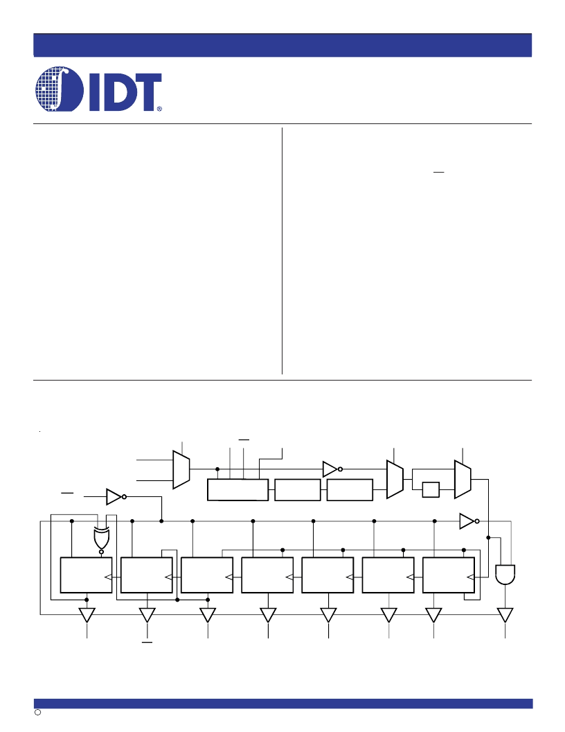
FUNCTIONAL BLOCK DIAGRAM
DESCRIPTION:
The QS5LV919 Clock Driver uses an internal phase locked loop
(PLL) to lock low skew outputs to one of two reference clock inputs.
Eight outputs are available: 2xQ, Q
0
-Q
4
, Q
5
, Q/2. Careful layout and
design ensure < 300 ps skew between the Q
0
-Q
4
, and Q/2 outputs.
The QS5LV919 includes an internal RC filter which provides excellent
jitter characteristics and elimnates the need for external components.
Various combinations of feedback and a divide-by-2 in the VCO path
allow applications to be customzed for linear VCO operation over a
wide range of input SYNC frequencies. The PLL can also be disabled
by the PLL_EN signal to allow low frequency or DC testing. The LOCK
output asserts to indicate when phase lock has been achieved. The
QS5LV919 is designed for use in high-performance workstations, multi-
board computers, networking hardware, and mainframe systems. Sev-
eral can be used in parallel or scattered throughout a systemfor guar-
anteed low skew, system-wide clock distribution networks.
For more information on PLL clock driver products, see Application
Note AN-227.
FEATURES:
3.3V operation
JEDEC compatible LVTTL level outputs
Clock inputs are 5V tolerant
< 300ps output skew, Q
0
–Q
4
2xQ output, Q outputs,
Q
output, Q/2 output
Outputs 3-state and reset while OE/
RST
low
PLL disable feature for low frequency testing
Internal loop filter RC network
Functional equivalent to MC88LV915, IDT74FCT388915
Positive or negative edge synchronization (
PE
)
Balanced drive outputs ±24mA
160MHz maximum frequency (2xQ output)
Available in QSOP and PLCC packages
The IDT logo is a registered trademark of Integrated Device Technology, Inc.
相關PDF資料 |
PDF描述 |
|---|---|
| QS5LV919100Q | 3.3V LOW SKEW CMOS PLL CLOCK DRIVER WITH INTEGRATED LOOP FILTER |
| QS5LV919133J | 3.3V LOW SKEW CMOS PLL CLOCK DRIVER WITH INTEGRATED LOOP FILTER |
| QS5LV931-50Q | 3.3V LOW SKEW CMOS PLL CLOCK DRIVER WITH INTEGRATED LOOP FILTER |
| QS5LV931-66Q | 3.3V LOW SKEW CMOS PLL CLOCK DRIVER WITH INTEGRATED LOOP FILTER |
| QS5LV931-80Q | 3.3V LOW SKEW CMOS PLL CLOCK DRIVER WITH INTEGRATED LOOP FILTER |
相關代理商/技術參數 |
參數描述 |
|---|---|
| QS5LV919100Q | 制造商:IDT 制造商全稱:Integrated Device Technology 功能描述:3.3V LOW SKEW CMOS PLL CLOCK DRIVER WITH INTEGRATED LOOP FILTER |
| QS5LV919-100Q | 制造商:Integrated Device Technology Inc 功能描述: 制造商:QSI 功能描述: |
| QS5LV919133J | 制造商:IDT 制造商全稱:Integrated Device Technology 功能描述:3.3V LOW SKEW CMOS PLL CLOCK DRIVER WITH INTEGRATED LOOP FILTER |
| QS5LV919133Q | 制造商:IDT 制造商全稱:Integrated Device Technology 功能描述:3.3V LOW SKEW CMOS PLL CLOCK DRIVER WITH INTEGRATED LOOP FILTER |
| QS5LV919-133Q | 制造商:Integrated Device Technology Inc 功能描述:PLL Clock Driver Single 28-Pin QSOP Tube |
發布緊急采購,3分鐘左右您將得到回復。