- 您現在的位置:買賣IC網 > PDF目錄192296 > S29CL032J1JFAI110 (SPANSION LLC) 1M X 32 FLASH 3.3V PROM, 54 ns, PBGA80 PDF資料下載
參數資料
| 型號: | S29CL032J1JFAI110 |
| 廠商: | SPANSION LLC |
| 元件分類: | PROM |
| 英文描述: | 1M X 32 FLASH 3.3V PROM, 54 ns, PBGA80 |
| 封裝: | 13 X 11 MM, 1 MM PITCH, FORTIFIED, BGA-80 |
| 文件頁數: | 66/78頁 |
| 文件大小: | 1825K |
| 代理商: | S29CL032J1JFAI110 |
第1頁第2頁第3頁第4頁第5頁第6頁第7頁第8頁第9頁第10頁第11頁第12頁第13頁第14頁第15頁第16頁第17頁第18頁第19頁第20頁第21頁第22頁第23頁第24頁第25頁第26頁第27頁第28頁第29頁第30頁第31頁第32頁第33頁第34頁第35頁第36頁第37頁第38頁第39頁第40頁第41頁第42頁第43頁第44頁第45頁第46頁第47頁第48頁第49頁第50頁第51頁第52頁第53頁第54頁第55頁第56頁第57頁第58頁第59頁第60頁第61頁第62頁第63頁第64頁第65頁當前第66頁第67頁第68頁第69頁第70頁第71頁第72頁第73頁第74頁第75頁第76頁第77頁第78頁
September 27, 2006 S29CD-J_CL-J_00_B1
S29CD-J & S29CL-J Flash Family
67
Pr el im i n a r y
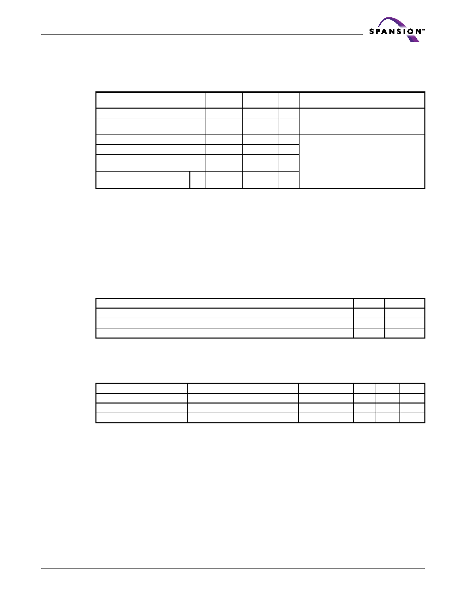
18.8 Erase and Programming Performance
Notes:
1. Typical program and erase times assume the following conditions: 25
°C, 2.5 V V
CC, 100K cycles. Additionally,
programming typicals assume checkerboard pattern.
2. Under worst case conditions of 145°C, VCC = 2.5 V, 1M cycles.
3. The typical chip programming time is considerably less than the maximum chip programming time listed.
4. In the pre-programming step of the Embedded Erase algorithm, all bytes are programmed to 00h before erasure.
5. System-level overhead is the time required to execute the two- or four-bus-cycle sequence for the program command.
See Table 20.1 and Table 20.2 for further information on command definitions.
6. PPBs have a program/erase cycle endurance of 100 cycles.
7. Guaranteed cycles per sector is 100K minimum.
18.9 Latchup Characteristics
Note: Includes all pins except VCC. Test conditions: VCC = 3.0 V, one pin at a time.
18.10 PQFP and Fortified BGA Pin Capacitance
Notes:
1. Sampled, not 100% tested.
2. Test conditions TA = 25°C, f = 1.0 MHz.
Table 18.6 Erase and Programming Performance
Parameter
Typ
Max
Unit
Comments
Sector Erase Time
0.5
5
s
Excludes 00h programming prior to erasure
Chip Erase Time
16 Mb = 46
32 Mb = 78
16 Mb = 230
32 Mb = 460
s
Double Word Program Time
8
130
s
Excludes system level overhead (Note 5)
Accelerated Double Word Program Time
8
130
s
Accelerated Chip Program Time
16 Mb = 5
32 Mb = 10
16 Mb = 50
32 Mb = 100
s
Chip Program Time (Note 3)
x32
16 Mb = 12
32 Mb = 24
16 Mb = 120
32 Mb = 240
s
Table 18.7 Latchup Characteristics
Description
Min
Max
Input voltage with respect to VSS on all pins except I/O pins (including A9, ACC, and WP#)
–1.0 V
12.5 V
Input voltage with respect to VSS on all I/O pins
–1.0 V
VCC + 1.0 V
VCC Current
–100 mA
+100 mA
Table 18.8 PQFP and Fortified BGA Pin Capacitance
Parameter Symbol
Parameter Description
Test Setup
Typ
Max
Unit
CIN
Input Capacitance
VIN = 0
6
7.5
pF
COUT
Output Capacitance
VOUT = 0
8.5
12
pF
CIN2
Control Pin Capacitance
VIN = 0
7.5
9
pF
相關PDF資料 |
PDF描述 |
|---|---|
| S29CL032J1MFAN120 | 1M X 32 FLASH 3.3V PROM, 54 ns, PBGA80 |
| S29CL032J0PQAN102 | 1M X 32 FLASH 3.3V PROM, 54 ns, PQFP80 |
| S29GL016A10FAI020 | 1M X 16 FLASH 3V PROM, 100 ns, PBGA64 |
| S29GL032A10TAIR10 | 64 MEGABIT 32MEGABIT 3.0 BOLT ONLY PAGE MODE FLASH MEMORY |
| S29GL032A10TAIR12 | 64 MEGABIT 32MEGABIT 3.0 BOLT ONLY PAGE MODE FLASH MEMORY |
相關代理商/技術參數 |
參數描述 |
|---|---|
| S29GL016A | 制造商:SPANSION 制造商全稱:SPANSION 功能描述:64 Megabit, 32 Megabit, and 16 Megabit 3.0-Volt only Page Mode Flash Memory Featuring 200 nm MirrorBit Process Technology |
| S29GL016A100BAI010 | 制造商:SPANSION 制造商全稱:SPANSION 功能描述:64 Megabit, 32 Megabit, and 16 Megabit 3.0-Volt only Page Mode Flash Memory Featuring 200 nm MirrorBit Process Technology |
| S29GL016A100BAI012 | 制造商:SPANSION 制造商全稱:SPANSION 功能描述:64 Megabit, 32 Megabit, and 16 Megabit 3.0-Volt only Page Mode Flash Memory Featuring 200 nm MirrorBit Process Technology |
| S29GL016A100BAI013 | 制造商:SPANSION 制造商全稱:SPANSION 功能描述:64 Megabit, 32 Megabit, and 16 Megabit 3.0-Volt only Page Mode Flash Memory Featuring 200 nm MirrorBit Process Technology |
| S29GL016A100BAIR10 | 制造商:SPANSION 制造商全稱:SPANSION 功能描述:64 Megabit, 32 Megabit, and 16 Megabit 3.0-Volt only Page Mode Flash Memory Featuring 200 nm MirrorBit Process Technology |
發布緊急采購,3分鐘左右您將得到回復。