- 您現在的位置:買賣IC網 > PDF目錄192296 > S29GL032M10BFIR12 (SPANSION LLC) MirrorBit Flash Family PDF資料下載
參數資料
| 型號: | S29GL032M10BFIR12 |
| 廠商: | SPANSION LLC |
| 元件分類: | PROM |
| 英文描述: | MirrorBit Flash Family |
| 中文描述: | 2M X 16 FLASH 3V PROM, 100 ns, PBGA64 |
| 封裝: | 13 X 11 MM, LEAD FREE, FORTIFIED BGA-64 |
| 文件頁數: | 17/158頁 |
| 文件大小: | 4695K |
| 代理商: | S29GL032M10BFIR12 |
第1頁第2頁第3頁第4頁第5頁第6頁第7頁第8頁第9頁第10頁第11頁第12頁第13頁第14頁第15頁第16頁當前第17頁第18頁第19頁第20頁第21頁第22頁第23頁第24頁第25頁第26頁第27頁第28頁第29頁第30頁第31頁第32頁第33頁第34頁第35頁第36頁第37頁第38頁第39頁第40頁第41頁第42頁第43頁第44頁第45頁第46頁第47頁第48頁第49頁第50頁第51頁第52頁第53頁第54頁第55頁第56頁第57頁第58頁第59頁第60頁第61頁第62頁第63頁第64頁第65頁第66頁第67頁第68頁第69頁第70頁第71頁第72頁第73頁第74頁第75頁第76頁第77頁第78頁第79頁第80頁第81頁第82頁第83頁第84頁第85頁第86頁第87頁第88頁第89頁第90頁第91頁第92頁第93頁第94頁第95頁第96頁第97頁第98頁第99頁第100頁第101頁第102頁第103頁第104頁第105頁第106頁第107頁第108頁第109頁第110頁第111頁第112頁第113頁第114頁第115頁第116頁第117頁第118頁第119頁第120頁第121頁第122頁第123頁第124頁第125頁第126頁第127頁第128頁第129頁第130頁第131頁第132頁第133頁第134頁第135頁第136頁第137頁第138頁第139頁第140頁第141頁第142頁第143頁第144頁第145頁第146頁第147頁第148頁第149頁第150頁第151頁第152頁第153頁第154頁第155頁第156頁第157頁第158頁
August 4, 2004 S29GLxxxM_00_B1_E
S29GLxxxM MirrorBitTM Flash Family
113
Da ta shee t
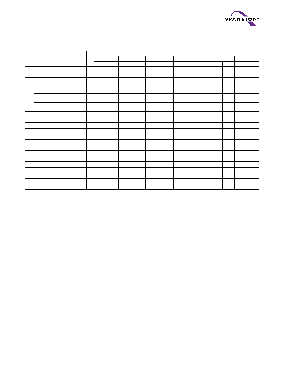
Command Definitions
Table 35. Command Definitions (x16 Mode, BYTE# = VIH)
Command
Sequence
(Note 1)
Cyc
le
s
Bus Cycles (Notes 2–5)
First
Second
Third
Fourth
Fifth
Sixth
Addr Data
Addr
Data
Addr
Data
Addr
Data
Addr
Data Addr Data
Read (Note 6)
1
RA
RD
Reset (Note 7)
1
XXX
F0
Au
to
se
le
ct
(
N
ot
e
8
)
Manufacturer ID
4
555
AA
2AA
55
555
90
X00
0001
Device ID (Note 9)
4
555
AA
2AA
55
555
90
X01
227E
X0E
X0F
SecSi‰ Sector Factory Protect
(Note 10)
4
555
AA
2AA
55
555
90
X03
(Note 10)
Sector Group Protect Verify (Note
12)
4
555
AA
2AA
55
555
90
(SA)X02
00/01
Enter SecSi Sector Region
3
555
AA
2AA
55
555
88
Exit SecSi Sector Region
4
555
AA
2AA
55
555
90
XXX
00
Program
4
555
AA
2AA
55
555
A0
PA
PD
Write to Buffer (Note 11)
3
555
AA
2AA
55
SA
25
SA
WC
PA
PD
WBL
PD
Program Buffer to Flash
1
SA
29
Write to Buffer Abort Reset (Note 13)
3
555
AA
2AA
55
555
F0
Unlock Bypass
3
555
AA
2AA
55
555
20
Unlock Bypass Program (Note 14)
2
XXX
A0
PA
PD
Unlock Bypass Reset (Note 15)
2
XXX
90
XXX
00
Chip Erase
6
555
AA
2AA
55
555
80
555
AA
2AA
55
555
10
Sector Erase
6
555
AA
2AA
55
555
80
555
AA
2AA
55
SA
30
Program/Erase Suspend (Note 16)
1
XXX
B0
Program/Erase Resume (Note 17)
1
XXX
30
CFI Query (Note 18)
1
55
98
Legend:
X = Don’t care
RA = Read Address of memory location to be read.
RD = Read Data read from location RA during read operation.
PA = Program Address. Addresses latch on falling edge of WE# or
CE# pulse, whichever happens later.
PD = Program Data for location PA. Data latches on rising edge of
WE# or CE# pulse, whichever happens first.
SA = Sector Address of sector to be verified (in autoselect mode) or
erased. Address bits A21–A15 uniquely select any sector.
WBL = Write Buffer Location. Address must be within same write
buffer page as PA.
WC = Word Count. Number of write buffer locations to load minus 1.
Notes:
1. See Table 1 for description of bus operations.
2. All values are in hexadecimal.
3. Shaded cells indicate read cycles. All others are write cycles.
4. During unlock and command cycles, when lower address bits are
555 or 2AA as shown in table, address bits above A11 and data
bits above DQ7 are don’t care.
5. No unlock or command cycles required when device is in read
mode.
6. Reset command is required to return to read mode (or to erase-
suspend-read mode if previously in Erase Suspend) when device
is in autoselect mode, or if DQ5 goes high while device is
providing status information.
7. Fourth cycle of the autoselect command sequence is a read
cycle. Data bits DQ15–DQ8 are don’t care. Except for RD, PD
and WC. See Autoselect Command Sequence section for more
information.
8. Device ID must be read in three cycles.
9. If WP# protects highest address sector, data is 98h for factory
locked and 18h for not factory locked. If WP# protects lowest
address sector, data is 88h for factory locked and 08h for not
factor locked.
10. Data is 00h for an unprotected sector group and 01h for a
protected sector group.
11. Total number of cycles in command sequence is determined by
number of words written to write buffer. Maximum number of
cycles in command sequence is 21, including “Program Buffer to
Flash” command.
12. Command sequence resets device for next command after
aborted write-to-buffer operation.
13. Unlock Bypass command is required prior to Unlock Bypass
Program command.
14. Unlock Bypass Reset command is required to return to read
mode when device is in unlock bypass mode.
15. System may read and program in non-erasing sectors, or enter
autoselect mode, when in Erase Suspend mode. Erase Suspend
command is valid only during a sector erase operation.
16. Erase Resume command is valid only during Erase Suspend
mode.
17. Command is valid when device is ready to read array data or
when device is in autoselect mode.
18. Refer to Table 18, AutoSelect Codes for individual Device IDs
per device density and model number.
相關PDF資料 |
PDF描述 |
|---|---|
| S29GL032M10BFIR13 | MirrorBit Flash Family |
| S29GL032M10BFIR30 | T528 Series - I, M, Z Case Sizes - Face Down Termination Tantalum Surface Mount Capacitor; Capacitance [nom]: 220uF; Working Voltage (Vdc)[max]: 6.3V; Capacitance Tolerance: +/-20%; Dielectric: Tantalum, Solid; ESR: 12mΩ; Lead Style: Surface-Mount Chip; Lead Dimensions: 7343-17; Termination: 100% Tin (Sn); Body Dimensions: 7.3mm x 4.3mm x 1.7mm; Temperature Range: -55C to +105C; Container: Tape & Reel; Qty per Container: 1,000; Features: Face Down Termination |
| S29GL032M10FAIR22 | MirrorBit Flash Family |
| S29GL032M10FAIR23 | MirrorBit Flash Family |
| S29GL032M10FAIR30 | MirrorBit Flash Family |
相關代理商/技術參數 |
參數描述 |
|---|---|
| S29GL032M10BFIR13 | 制造商:SPANSION 制造商全稱:SPANSION 功能描述:3.0 Volt-only Page Mode Flash Memory featuring 0.23 um MirrorBit process technology |
| S29GL032M10BFIR20 | 制造商:SPANSION 制造商全稱:SPANSION 功能描述:MirrorBit Flash Family |
| S29GL032M10BFIR22 | 制造商:SPANSION 制造商全稱:SPANSION 功能描述:MirrorBit Flash Family |
| S29GL032M10BFIR23 | 制造商:SPANSION 制造商全稱:SPANSION 功能描述:MirrorBit Flash Family |
| S29GL032M10BFIR30 | 制造商:SPANSION 制造商全稱:SPANSION 功能描述:3.0 Volt-only Page Mode Flash Memory featuring 0.23 um MirrorBit process technology |
發布緊急采購,3分鐘左右您將得到回復。