- 您現在的位置:買賣IC網 > PDF目錄374788 > SI5364 (Electronic Theatre Controls, Inc.) SONET/SDH PRECISION PORT CARD CLOCK IC PDF資料下載
參數資料
| 型號: | SI5364 |
| 廠商: | Electronic Theatre Controls, Inc. |
| 英文描述: | SONET/SDH PRECISION PORT CARD CLOCK IC |
| 中文描述: | SONET / SDH的精密端口卡時鐘IC |
| 文件頁數: | 1/40頁 |
| 文件大小: | 565K |
| 代理商: | SI5364 |
當前第1頁第2頁第3頁第4頁第5頁第6頁第7頁第8頁第9頁第10頁第11頁第12頁第13頁第14頁第15頁第16頁第17頁第18頁第19頁第20頁第21頁第22頁第23頁第24頁第25頁第26頁第27頁第28頁第29頁第30頁第31頁第32頁第33頁第34頁第35頁第36頁第37頁第38頁第39頁第40頁
Rev. 2.2 7/04
Copyright 2004 by Silicon Laboratories
Si5364
Si5364
SONET/SDH P
RECISION
P
ORT
C
ARD
C
LOCK
IC
Features
Applications
Description
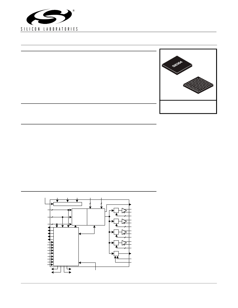
The Si5364 is a complete solution for ultra-low jitter high-speed clock generation and
distribution in precision clocking applications, such as OC-192/OC-48 SONET/SDH line/
port cards. This device phase locks to one of three reference inputs in the range of
19.44 MHz and generates four synchronous clock outputs that can be independently
configured for operation in the 19, 155, or 622 MHz range (1, 8, and 32x input clock).
Silicon Laboratories DSPLL technology delivers phase-locked loop (PLL) functionality
with unparalleled performance while eliminating external loop filter components,
providing programmable loop parameters, and simplifying design. The on-chip reference
monitoring and clock switching functions support Stratum 3/3E and SMC compatible
clock switching with excellent output phase transient characteristics. FEC rates are
supported with selectable 255/238 or 238/255 scaling of the clock multiplication ratios.
The Si5364 establishes a new standard in performance and integration for ultra-low jitter
clock generation. It operates from a single 3.3 V supply.
Functional Block Diagram
Ultra-low jitter clock outputs with jitter
generation as low as 0.3 ps
RMS
No external components (other than a
resistor and standard bypassing)
Up to three clock inputs
Four independent clock outputs at 19,
155, or 622 MHz
Stratum 3, 3E, and SMC compatible
Digital hold for loss-of-input clock
Automatic or manually-controlled hitless
switching between clock inputs
Revertive/non-revertive switching
Loss-of-signal and frequency offset
alarms for each clock input
Support for forward and reverse FEC
clock scaling
8 kHz frame sync output
Low power
Small size (11x11 mm)
SONET/SDH line/port cards
Terabit routers
Core switches
Digital cross connects
FRQSEL_1[1:0]
CLKOUT_1+
CLKOUT_1–
2
2
2
2
DSBLFSYNC
FSYNC
MANCNTRL[1:0]
VALTIME
AUTOSEL
RVRT
A_ACTV
B_ACTV
LOS_A
FOS_A
LOS_B
FOS_B
LOS_F
DSBLFOS
REF/CLKIN_F+
REF/CLKIN_F–
CLKIN_B+
CLKIN_B–
CLKIN_A+
CLKIN_A–
CAL_ACTV
Signal
Detection,
Selection,
& Control
2
2
2
SMC/S3N
F_ACTV
DH_ACTV
RSTN/CAL
FEC[1:0]
BWSEL[1:0]
2
CLKOUT_2+
CLKOUT_2–
CLKOUT_3+
CLKOUT_3–
CLKOUT_4+
CLKOUT_4–
FRQSEL_2[1:0]
FRQSEL_3[1:0]
FRQSEL_4[1:0]
SYNCIN
Biasing & Supply
REXT
VSEL33
VDD
GND
÷
÷
÷
÷
÷
2
SiLECT
TM
Switching
DSPLL
TM
FXDDELAY
INCDELAY
DECDELAY
Ordering Information:
See page 36.
Si5364
Bottom View
相關PDF資料 |
PDF描述 |
|---|---|
| SI5364-F-BC | SONET/SDH PRECISION PORT CARD CLOCK IC |
| SI5600 | SiPHY-TM OC-192/STM-64 SONET/SDH TRANSCEIVER |
| SI5600-BC | SiPHY-TM OC-192/STM-64 SONET/SDH TRANSCEIVER |
| SI7661 | HEATSINK TO-202 CLIP-ON .58 BK |
| SI7661DJ | HEATSINK TO-220 CLIP-ON BLK |
相關代理商/技術參數 |
參數描述 |
|---|---|
| SI5364BC | 制造商:SILICON 功能描述: |
| SI5364-EVB | 功能描述:時鐘和定時器開發工具 Multi/Jitter/Hitless 19 55 622MHz Out RoHS:否 制造商:Texas Instruments 產品:Evaluation Modules 類型:Clock Conditioners 工具用于評估:LMK04100B 頻率:122.8 MHz 工作電源電壓:3.3 V |
| SI5364FBC | 制造商:Vishay Siliconix 功能描述: |
| SI5364-F-BC | 功能描述:時鐘合成器/抖動清除器 Multi/Jitter/Hitless 19 55 622MHz Outpt RoHS:否 制造商:Skyworks Solutions, Inc. 輸出端數量: 輸出電平: 最大輸出頻率: 輸入電平: 最大輸入頻率:6.1 GHz 電源電壓-最大:3.3 V 電源電壓-最小:2.7 V 封裝 / 箱體:TSSOP-28 封裝:Reel |
| SI5364-G-BC | 功能描述:時鐘發生器及支持產品 SONET/SDH Precision Port Card 19 155 622 RoHS:否 制造商:Silicon Labs 類型:Clock Generators 最大輸入頻率:14.318 MHz 最大輸出頻率:166 MHz 輸出端數量:16 占空比 - 最大:55 % 工作電源電壓:3.3 V 工作電源電流:1 mA 最大工作溫度:+ 85 C 安裝風格:SMD/SMT 封裝 / 箱體:QFN-56 |
發布緊急采購,3分鐘左右您將得到回復。