- 您現(xiàn)在的位置:買賣IC網(wǎng) > PDF目錄98216 > THS10064CDA (TEXAS INSTRUMENTS INC) 4-CH 10-BIT PROPRIETARY METHOD ADC, PARALLEL ACCESS, PDSO32 PDF資料下載
參數(shù)資料
| 型號: | THS10064CDA |
| 廠商: | TEXAS INSTRUMENTS INC |
| 元件分類: | ADC |
| 英文描述: | 4-CH 10-BIT PROPRIETARY METHOD ADC, PARALLEL ACCESS, PDSO32 |
| 封裝: | GREEN, PLASTIC, TSSOP-32 |
| 文件頁數(shù): | 39/42頁 |
| 文件大小: | 527K |
| 代理商: | THS10064CDA |
第1頁第2頁第3頁第4頁第5頁第6頁第7頁第8頁第9頁第10頁第11頁第12頁第13頁第14頁第15頁第16頁第17頁第18頁第19頁第20頁第21頁第22頁第23頁第24頁第25頁第26頁第27頁第28頁第29頁第30頁第31頁第32頁第33頁第34頁第35頁第36頁第37頁第38頁當前第39頁第40頁第41頁第42頁
THS10064
SLAS255B – DECEMBER 1999 – REVISED DECEMBER 2002
www.ti.com
6
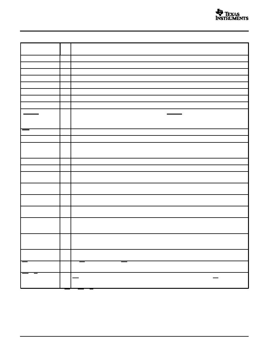
Terminal Functions
TERMINAL
I/O
DESCRIPTION
NAME
NO.
I/O
DESCRIPTION
AINP
32
I
Analog input, single-ended or positive input of differential channel A
AINM
31
I
Analog input, single-ended or negative input of differential channel A
BINP
30
I
Analog input, single-ended or positive input of differential channel B
BINM
29
I
Analog input, single-ended or negative input of differential channel B
AVDD
23
I
Analog supply voltage
AGND
24
I
Analog ground
BVDD
7
I
Digital supply voltage for buffer
BGND
8
I
Digital ground for buffer
CONV_CLK
(CONVST)
15
I
Digital input. This input is used to apply an external conversion clock in continuous conversion mode. In single
conversion mode, this input functions as the conversion start (CONVST) input. A high to low transition on this input
holds simultaneously the selected analog input channels and initiates a single conversion of all selected analog
inputs.
CS0
22
I
Chip select input (active low)
CS1
21
I
Chip select input (active high)
DATA_AV
16
O
Data available signal, which can be used to generate an interrupt for processors and as a level information of the
internal FIFO. This signal can be configured to be active low or high and can be configured as a static level or pulse
output. See Table 14.
DGND
17
I
Digital ground. Ground reference for digital circuitry.
DVDD
18
I
Digital supply voltage
D0 – D9
1–6,
9–12
I/
O/Z
Digital input, output; D0 = LSB
RA0
13
I
Digital input. RA0 is used as an address line for the control register. This is required for writing to the control
register 0 and control register 1. See Table 8.
RA1
14
I
Digital input. RA1 is used as an address line for the control register. This is required for writing to control register 0
and control register 1. See Table 8.
REFIN
28
I
Common-mode reference input for the analog input channels. It is recommended that this pin be connected to the
reference output REFOUT.
REFP
26
I
Reference input, requires a bypass capacitor of 10
F to AGND in order to bypass the internal reference voltage.
An external reference voltage at this input can be applied. This option can be programmed through control
register 0. See Table 9.
REFM
25
I
Reference input, requires a bypass capacitor of 10
F to AGND in order to bypass the internal reference voltage.
An external reference voltage at this input can be applied. This option can be programmed through control
register 0. See Table 9.
REFOUT
27
O
Analog fixed reference output voltage of 2.5 V. Sink and source capability of 250
A.Thereferenceoutputrequires
a capacitor of 10
F to AGND for filtering and stability.
RD
19
I
The RD input is used only if the WR input is configured as a write only input. In this case, it is a digital input, active
low as a data read select from the processor. See timing section.
WR (R/W)
20
I
This input is programmable. It functions as a read-write input R/W and can also be configured as a write-only input
WR, which is active low and used as data write select from the processor. In this case, the RD input is used as a
read input from the processor. See timing section.
(1) The start-conditions of RD and WR (R/W) are unknown. The first access to the ADC has to be a write access to initialize the ADC.
相關(guān)PDF資料 |
PDF描述 |
|---|---|
| THS10064IDA | 4-CH 10-BIT PROPRIETARY METHOD ADC, PARALLEL ACCESS, PDSO32 |
| THS10064CDAR | 4-CH 10-BIT PROPRIETARY METHOD ADC, PARALLEL ACCESS, PDSO32 |
| THS10064IDAR | 4-CH 10-BIT PROPRIETARY METHOD ADC, PARALLEL ACCESS, PDSO32 |
| THS10064IDAG4 | 4-CH 10-BIT PROPRIETARY METHOD ADC, PARALLEL ACCESS, PDSO32 |
| THS1007CDA | 4-CH 10-BIT PROPRIETARY METHOD ADC, PARALLEL ACCESS, PDSO32 |
相關(guān)代理商/技術(shù)參數(shù) |
參數(shù)描述 |
|---|---|
| THS10064CDAG4 | 功能描述:模數(shù)轉(zhuǎn)換器 - ADC 10-Bit 6 MSPS Quad Ch DSP/uP Ifc RoHS:否 制造商:Texas Instruments 通道數(shù)量:2 結(jié)構(gòu):Sigma-Delta 轉(zhuǎn)換速率:125 SPs to 8 KSPs 分辨率:24 bit 輸入類型:Differential 信噪比:107 dB 接口類型:SPI 工作電源電壓:1.7 V to 3.6 V, 2.7 V to 5.25 V 最大工作溫度:+ 85 C 安裝風格:SMD/SMT 封裝 / 箱體:VQFN-32 |
| THS10064CDAR | 功能描述:模數(shù)轉(zhuǎn)換器 - ADC 10-Bit 6 MSPS Quad Ch DSP/uP Ifc RoHS:否 制造商:Texas Instruments 通道數(shù)量:2 結(jié)構(gòu):Sigma-Delta 轉(zhuǎn)換速率:125 SPs to 8 KSPs 分辨率:24 bit 輸入類型:Differential 信噪比:107 dB 接口類型:SPI 工作電源電壓:1.7 V to 3.6 V, 2.7 V to 5.25 V 最大工作溫度:+ 85 C 安裝風格:SMD/SMT 封裝 / 箱體:VQFN-32 |
| THS10064CDARG4 | 功能描述:模數(shù)轉(zhuǎn)換器 - ADC 10-Bit 6 MSPS Quad Ch DSP/uP Ifc RoHS:否 制造商:Texas Instruments 通道數(shù)量:2 結(jié)構(gòu):Sigma-Delta 轉(zhuǎn)換速率:125 SPs to 8 KSPs 分辨率:24 bit 輸入類型:Differential 信噪比:107 dB 接口類型:SPI 工作電源電壓:1.7 V to 3.6 V, 2.7 V to 5.25 V 最大工作溫度:+ 85 C 安裝風格:SMD/SMT 封裝 / 箱體:VQFN-32 |
| THS10064DA | 制造商:TI 制造商全稱:Texas Instruments 功能描述:10-BIT 6 MSPS, SIMULTANEOUS SAMPLING ANALOG-TO-DIGITAL CONVERTER |
| THS10064EVM | 制造商:Texas Instruments 功能描述:THS10064 10-BIT, 6 MSPS, DC EVM - Bulk |
發(fā)布緊急采購,3分鐘左右您將得到回復。