- 您現在的位置:買賣IC網 > PDF目錄98223 > THS3125CPWPG4 (TEXAS INSTRUMENTS INC) 1 CHANNEL, VIDEO AMPLIFIER, PDSO14 PDF資料下載
參數資料
| 型號: | THS3125CPWPG4 |
| 廠商: | TEXAS INSTRUMENTS INC |
| 元件分類: | 音頻/視頻放大 |
| 英文描述: | 1 CHANNEL, VIDEO AMPLIFIER, PDSO14 |
| 封裝: | GREEN, PLASTIC, HTSSOP-14 |
| 文件頁數: | 7/34頁 |
| 文件大小: | 1276K |
| 代理商: | THS3125CPWPG4 |
第1頁第2頁第3頁第4頁第5頁第6頁當前第7頁第8頁第9頁第10頁第11頁第12頁第13頁第14頁第15頁第16頁第17頁第18頁第19頁第20頁第21頁第22頁第23頁第24頁第25頁第26頁第27頁第28頁第29頁第30頁第31頁第32頁第33頁第34頁
SLOS382D
– SEPTEMBER 2001 – REVISED FEBRUARY 2011
Power-Down Reference Pin Operation
Printed-Circuit Board Layout Techniques for
Optimal Performance
In addition to the shutdown pin, the THS3125
features a reference pin (REF) which allows the user
Achieving optimum performance with high-frequency
to control the enable or disable power-down voltage
amplifiers such as the THS3125 and THS3122
levels applied to the SHUTDOWN pin. In most
requires careful attention to board layout parasitic and
split-supply
applications,
the
reference
pin
is
external component types. Recommendations that
connected to ground. In either case, the user must be
optimize performance include:
aware of voltage-level thresholds that apply to the
Minimize parasitic capacitance to any ac ground
shutdown pin. Table 2 shows examples and illustrate
for all of the signal I/O pins. Parasitic capacitance
the relationship between the reference voltage and
on the output and input pins can cause instability.
the power-down thresholds. In the table, the threshold
To reduce unwanted capacitance, a window
levels are derived by the following equations:
around the signal I/O pins should be opened in all
of the ground and power planes around those
SHUTDOWN
≤ REF + 0.8 V for enable
pins. Otherwise, ground and power planes should
SHUTDOWN
≥ REF + 2V for disable
be unbroken elsewhere on the board.
Where the usable range at the REF pin is:
Minimize the distance [0.25 inch, (6,4 mm)] from
the power-supply pins to high-frequency 0.1-
F
VCC– ≤ VREF ≤ (VCC+ – 4V)
and 100-pF decoupling capacitors. At the device
The recommended mode of operation is to tie the
pins, the ground and power plane layout should
REF
pin
to
midrail,
therefore
setting
the
not be in close proximity to the signal I/O pins.
enable/disable thresholds to V(midrail) + 0.8 V and
Avoid
narrow
power
and
ground
traces
to
V(midrail) = 2 V, respectively.
minimize inductance between the pins and the
decoupling
capacitors.
The
power-supply
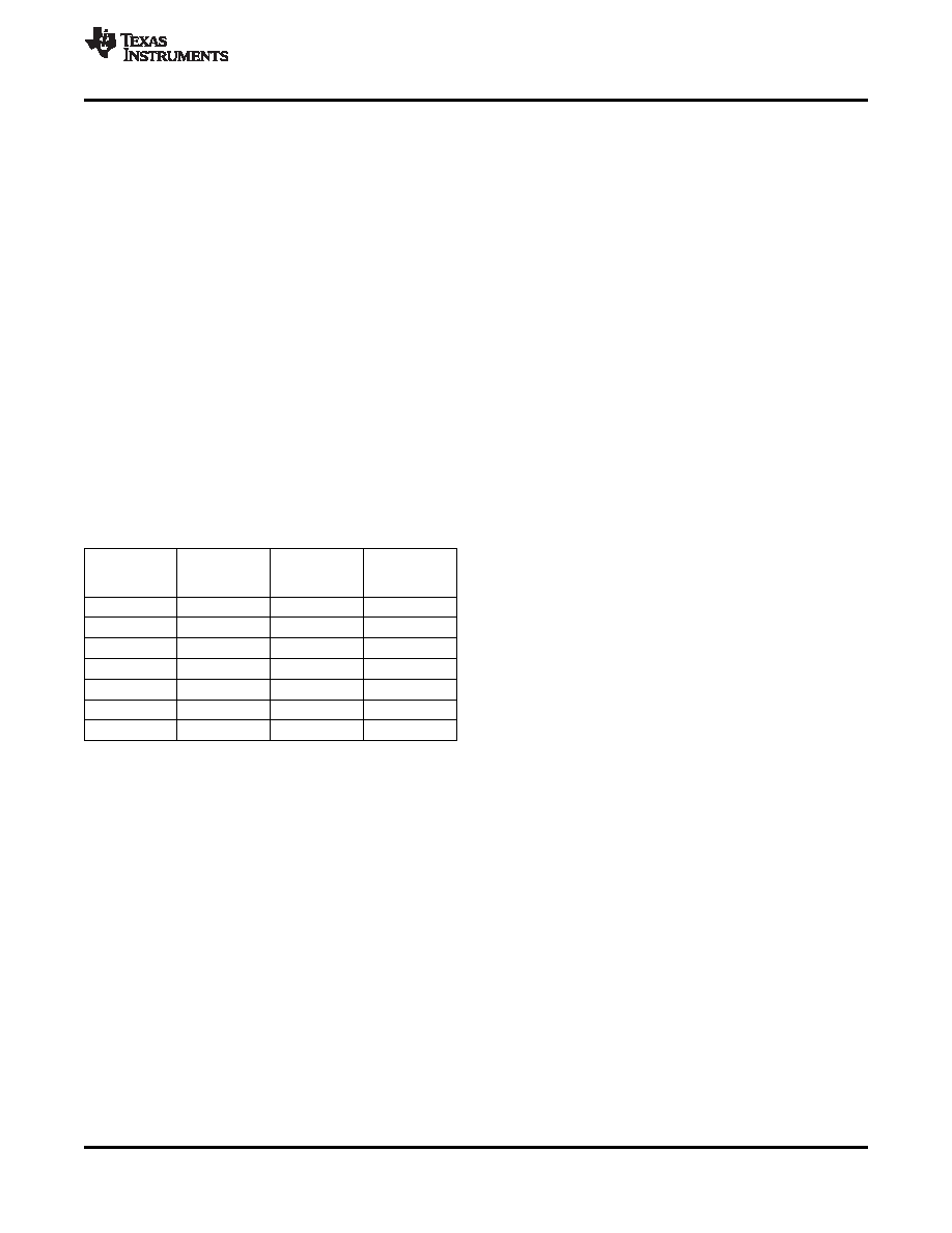
Table 2. Shutdown Threshold Voltage Levels
connections should always be decoupled with
these
capacitors.
Larger
(6.8
F
or
more)
REFERENCE
tantalum decoupling capacitors, effective at lower
SUPPLY
PIN
ENABLE
DISABLE
frequencies, should also be used on the main
VOLTAGE (V)
LEVEL (V)
supply pins. These capacitors may be placed
±15, ±5
0
0.8
2.0
somewhat farther from the device and may be
±15
2.0
2.8
4.0
shared among several devices in the same area
±15
–2.0
–1.2
0
of the printed circuit board (PCB).
±5
1.0
1.8
3.0
Careful
selection
and
placement
of
external
±5
–1.0
–0.2
1.0
components
preserve
the
high-frequency
+30
15.0
15.8
17
performance of the THS3125 and THS3122.
Resistors should be a very low reactance type.
+10
5.0
5.8
7.0
Surface-mount resistors work best and allow a
tighter overall layout. Again, keep the leads and
Note that if the REF pin is left unterminated, it floats
PCB trace length as short as possible. Never use
to
the
positive
rail
and
falls
outside
of
the
wirebound type resistors in a high-frequency
recommended operating range given above VCC– ≤
application. Because the output pin and inverting
VREF ≤ (VCC+ – 4V). As a result, it no longer serves as
input pins are the most sensitive to parasitic
a reliable reference for the SHUTDOWN pin, and the
capacitance, always position the feedback and
enable/disable thresholds given above no longer
series output resistors, if any, as close as possible
apply.
If
the
SHUTDOWN
pin
is
also
left
to the inverting input pins and output pins. Other
unterminated, it floats to the positive rail and the
network components, such as input termination
device is disabled. If balanced, split supplies are used
resistors,
should
be
placed
close
to
the
(
±VS) and the REF and SHUTDOWN pins are
gain-setting resistors. Even with a low parasitic
grounded, the device is enabled.
capacitance that shunts the external resistors,
space
excessively
high
resistor
values
can
create
significant
time
constants
that
can
degrade
space
performance.
Good
axial
metal-film
or
space
surface-mount resistors have approximately 0.2
pF in shunt with the resistor. For resistor values
greater than 2.0 k
Ω, this parasitic capacitance can
add a pole and/or a zero that can affect circuit
operation.
Keep
resistor
values
as
low
as
possible,
consistent
with
load
driving
considerations.
2001–2011, Texas Instruments Incorporated
15
相關PDF資料 |
PDF描述 |
|---|---|
| THS3125IPWPG4 | 1 CHANNEL, VIDEO AMPLIFIER, PDSO14 |
| THS3125IPWPRG4 | 1 CHANNEL, VIDEO AMPLIFIER, PDSO14 |
| THS3122CDDARG3 | 1 CHANNEL, VIDEO AMPLIFIER, PDSO8 |
| THS3125CDG4 | 1 CHANNEL, VIDEO AMPLIFIER, PDSO14 |
| THS3125CDRG4 | 1 CHANNEL, VIDEO AMPLIFIER, PDSO14 |
相關代理商/技術參數 |
參數描述 |
|---|---|
| THS3125CPWPR | 功能描述:高速運算放大器 Dual High Output Current 120-MHz RoHS:否 制造商:Texas Instruments 通道數量:1 電壓增益 dB:116 dB 輸入補償電壓:0.5 mV 轉換速度:55 V/us 工作電源電壓:36 V 電源電流:7.5 mA 最大工作溫度:+ 85 C 安裝風格:SMD/SMT 封裝 / 箱體:SOIC-8 封裝:Tube |
| THS3125CPWPRG4 | 功能描述:高速運算放大器 Dual High Output Current 120-MHz RoHS:否 制造商:Texas Instruments 通道數量:1 電壓增益 dB:116 dB 輸入補償電壓:0.5 mV 轉換速度:55 V/us 工作電源電壓:36 V 電源電流:7.5 mA 最大工作溫度:+ 85 C 安裝風格:SMD/SMT 封裝 / 箱體:SOIC-8 封裝:Tube |
| THS3125EVM | 功能描述:放大器 IC 開發工具 THS3125 Eval Mod RoHS:否 制造商:International Rectifier 產品:Demonstration Boards 類型:Power Amplifiers 工具用于評估:IR4302 工作電源電壓:13 V to 23 V |
| THS3125ID | 功能描述:高速運算放大器 Dual High Output Current 120-MHz RoHS:否 制造商:Texas Instruments 通道數量:1 電壓增益 dB:116 dB 輸入補償電壓:0.5 mV 轉換速度:55 V/us 工作電源電壓:36 V 電源電流:7.5 mA 最大工作溫度:+ 85 C 安裝風格:SMD/SMT 封裝 / 箱體:SOIC-8 封裝:Tube |
| THS3125IDG4 | 功能描述:高速運算放大器 Dual High Output Current 120-MHz RoHS:否 制造商:Texas Instruments 通道數量:1 電壓增益 dB:116 dB 輸入補償電壓:0.5 mV 轉換速度:55 V/us 工作電源電壓:36 V 電源電流:7.5 mA 最大工作溫度:+ 85 C 安裝風格:SMD/SMT 封裝 / 箱體:SOIC-8 封裝:Tube |
發布緊急采購,3分鐘左右您將得到回復。