- 您現在的位置:買賣IC網 > PDF目錄98223 > THS3125CPWPG4 (TEXAS INSTRUMENTS INC) 1 CHANNEL, VIDEO AMPLIFIER, PDSO14 PDF資料下載
參數資料
| 型號: | THS3125CPWPG4 |
| 廠商: | TEXAS INSTRUMENTS INC |
| 元件分類: | 音頻/視頻放大 |
| 英文描述: | 1 CHANNEL, VIDEO AMPLIFIER, PDSO14 |
| 封裝: | GREEN, PLASTIC, HTSSOP-14 |
| 文件頁數: | 8/34頁 |
| 文件大小: | 1276K |
| 代理商: | THS3125CPWPG4 |
第1頁第2頁第3頁第4頁第5頁第6頁第7頁當前第8頁第9頁第10頁第11頁第12頁第13頁第14頁第15頁第16頁第17頁第18頁第19頁第20頁第21頁第22頁第23頁第24頁第25頁第26頁第27頁第28頁第29頁第30頁第31頁第32頁第33頁第34頁
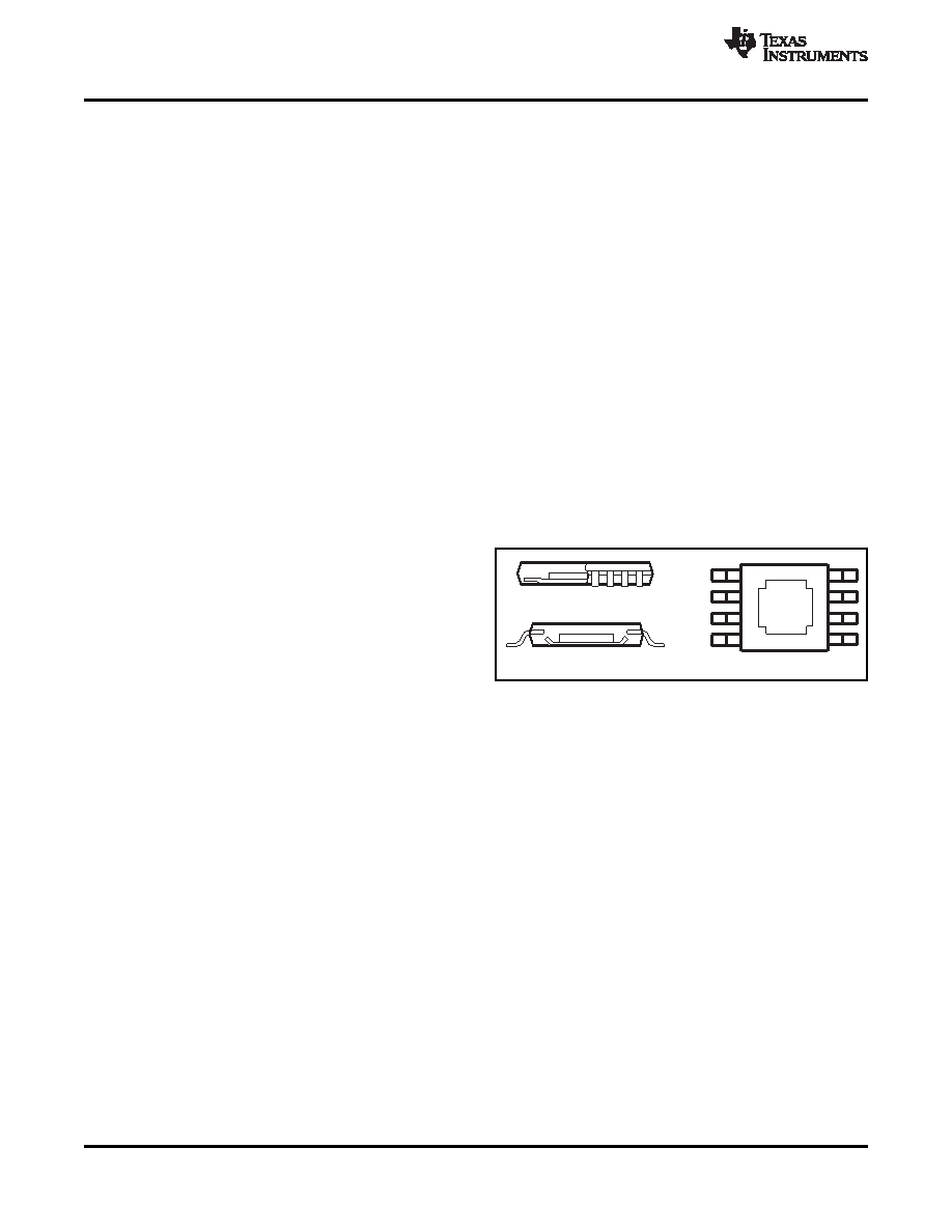
DIE
Thermal
Pad
(a) SideView
(c) BottomView
(b) EndView
SLOS382D
– SEPTEMBER 2001 – REVISED FEBRUARY 2011
Connections to other wideband devices on the
Socketing a high-speed device such as the
board may be made with short direct traces or
THS3125 and THS3122 is not recommended. The
through onboard transmission lines. For short
additional lead length and pin-to-pin capacitance
connections, consider the trace and the input to
introduced by the socket can create an extremely
the next device as a lumped capacitive load.
troublesome parasitic network which can make it
Relatively wide traces [0.05 inch (1,3 mm) to 0.1
almost impossible to achieve a smooth, stable
inch (2,54 mm)] should be used, preferably with
frequency response. Best results are obtained by
ground and power planes opened up around
soldering
the
THS3125/THS3122
amplifiers
them. Estimate the total capacitive load and
directly onto the board.
determine if isolation resistors on the outputs are
necessary. Low parasitic capacitive loads (less
PowerPAD
Design Considerations
than 4 pF) may not need an RS because the
The THS3125 and THS3122 are available in a
THS3125
and
THS3122
are
nominally
thermally-enhanced PowerPAD family of packages.
compensated to operate with a 2-pF parasitic
These packages are constructed using a downset
load. Higher parasitic capacitive loads without an
leadframe upon which the die is mounted [see
RS are allowed as the signal gain increases (thus
Figure 48(a) and Figure 48(b)]. This arrangement
increasing the unloaded phase margin). If a long
results in the lead frame being exposed as a thermal
trace is required, and the 6-dB signal loss intrinsic
pad
on
the
underside
of
the
package
[see
to
a
doubly-terminated
transmission
line
is
Figure 48(c)]. Because this thermal pad has direct
acceptable,
implement
a
matched-impedance
thermal contact with the die, excellent thermal
transmission line using microstrip or stripline
performance can be achieved by providing a good
techniques (consult an ECL design handbook for
thermal path away from the thermal pad. Note that
microstrip and stripline layout techniques). A 50-
Ω
devices such as the THS312x have no electrical
environment is not necessary onboard, and in
connection between the PowerPAD and the die.
fact, a higher impedance environment improves
distortion as shown in the distortion versus load
plots. With a characteristic board trace impedance
based on board material and trace dimensions, a
matching series resistor into the trace from the
output of the THS3125/THS3122 is used as well
as a terminating shunt resistor at the input of the
destination
device.
Remember
also
that
the
terminating impedance is the parallel combination
of the shunt resistor and the input impedance of
Figure 48. Views of Thermally-Enhanced Package
the
destination
device:
this
total
effective
impedance should be set to match the trace
impedance.
If
the
6-dB
attenuation
of
a
The PowerPAD package allows for both assembly
doubly-terminated
transmission
line
is
and thermal management in one manufacturing
unacceptable,
a
long
trace
can
be
operation. During the surface-mount solder operation
series-terminated at the source end only. Treat
(when the leads are being soldered), the thermal pad
the trace as a capacitive load in this case. This
can also be soldered to a copper area underneath the
configuration does not preserve signal integrity as
package. Through the use of thermal paths within this
well as a doubly-terminated line. If the input
copper area, heat can be conducted away from the
impedance of the destination device is low, there
package into either a ground plane or other heat
is some signal attenuation as a result of the
dissipating device.
voltage divider formed by the series output into
The PowerPAD package represents a breakthrough
the terminating impedance.
in combining the small area and ease of assembly of
surface
mount
with
the,
heretofore,
awkward
mechanical methods of heatsinking.
16
2001–2011, Texas Instruments Incorporated
相關PDF資料 |
PDF描述 |
|---|---|
| THS3125IPWPG4 | 1 CHANNEL, VIDEO AMPLIFIER, PDSO14 |
| THS3125IPWPRG4 | 1 CHANNEL, VIDEO AMPLIFIER, PDSO14 |
| THS3122CDDARG3 | 1 CHANNEL, VIDEO AMPLIFIER, PDSO8 |
| THS3125CDG4 | 1 CHANNEL, VIDEO AMPLIFIER, PDSO14 |
| THS3125CDRG4 | 1 CHANNEL, VIDEO AMPLIFIER, PDSO14 |
相關代理商/技術參數 |
參數描述 |
|---|---|
| THS3125CPWPR | 功能描述:高速運算放大器 Dual High Output Current 120-MHz RoHS:否 制造商:Texas Instruments 通道數量:1 電壓增益 dB:116 dB 輸入補償電壓:0.5 mV 轉換速度:55 V/us 工作電源電壓:36 V 電源電流:7.5 mA 最大工作溫度:+ 85 C 安裝風格:SMD/SMT 封裝 / 箱體:SOIC-8 封裝:Tube |
| THS3125CPWPRG4 | 功能描述:高速運算放大器 Dual High Output Current 120-MHz RoHS:否 制造商:Texas Instruments 通道數量:1 電壓增益 dB:116 dB 輸入補償電壓:0.5 mV 轉換速度:55 V/us 工作電源電壓:36 V 電源電流:7.5 mA 最大工作溫度:+ 85 C 安裝風格:SMD/SMT 封裝 / 箱體:SOIC-8 封裝:Tube |
| THS3125EVM | 功能描述:放大器 IC 開發工具 THS3125 Eval Mod RoHS:否 制造商:International Rectifier 產品:Demonstration Boards 類型:Power Amplifiers 工具用于評估:IR4302 工作電源電壓:13 V to 23 V |
| THS3125ID | 功能描述:高速運算放大器 Dual High Output Current 120-MHz RoHS:否 制造商:Texas Instruments 通道數量:1 電壓增益 dB:116 dB 輸入補償電壓:0.5 mV 轉換速度:55 V/us 工作電源電壓:36 V 電源電流:7.5 mA 最大工作溫度:+ 85 C 安裝風格:SMD/SMT 封裝 / 箱體:SOIC-8 封裝:Tube |
| THS3125IDG4 | 功能描述:高速運算放大器 Dual High Output Current 120-MHz RoHS:否 制造商:Texas Instruments 通道數量:1 電壓增益 dB:116 dB 輸入補償電壓:0.5 mV 轉換速度:55 V/us 工作電源電壓:36 V 電源電流:7.5 mA 最大工作溫度:+ 85 C 安裝風格:SMD/SMT 封裝 / 箱體:SOIC-8 封裝:Tube |
發布緊急采購,3分鐘左右您將得到回復。