- 您現在的位置:買賣IC網 > PDF目錄98226 > THS4271DRB (TEXAS INSTRUMENTS INC) VIDEO AMPLIFIER, PDSO8 PDF資料下載
參數資料
| 型號: | THS4271DRB |
| 廠商: | TEXAS INSTRUMENTS INC |
| 元件分類: | 音頻/視頻放大 |
| 英文描述: | VIDEO AMPLIFIER, PDSO8 |
| 封裝: | EXPOSED PAD, LEADLESS, PLASTIC, MSOP-8 |
| 文件頁數: | 20/35頁 |
| 文件大小: | 422K |
| 代理商: | THS4271DRB |
第1頁第2頁第3頁第4頁第5頁第6頁第7頁第8頁第9頁第10頁第11頁第12頁第13頁第14頁第15頁第16頁第17頁第18頁第19頁當前第20頁第21頁第22頁第23頁第24頁第25頁第26頁第27頁第28頁第29頁第30頁第31頁第32頁第33頁第34頁第35頁
THS4271
THS4275
SLOS397C – JULY 2002 – REVISED JANUARY 2003
www.ti.com
27
6.
The top-side solder mask should leave the terminals
of the package and the thermal pad area with its five
holes exposed. The bottom-side solder mask should
cover the five holes of the thermal pad area. This
prevents solder from being pulled away from the
thermal pad area during the reflow process.
7.
Apply solder paste to the exposed thermal pad area
and all of the IC terminals.
8.
With these preparatory steps in place, the IC is simply
placed in position and run through the solder reflow
operation
as
any
standard
surface-mount
component. This results in a part that is properly
installed.
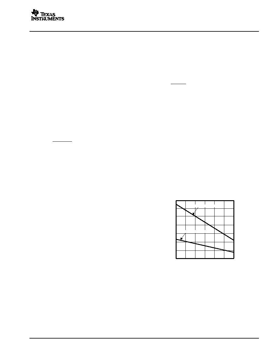
For a given
θJA , the maximum power dissipation is shown
in Figure 91 and is calculated by the equation 5:
P
D +
Tmax
* T
A
q
JA
where:
PD = Maximum power dissipation of THS4271 (watts)
TMAX = Absolute maximum junction temperature (150°C)
TA = Free-ambient temperature (°C)
θJA = θJC + θCA
θJC = Thermal coefficient from junction to the case
θCA = Thermal coefficient from the case to ambient air
(
°C/W).
The next consideration is the package constraints. The
two sources of heat within an amplifier are quiescent
power and output power. The designer should never forget
about the quiescent heat generated within the device,
especially multi-amplifier devices. Because these devices
have linear output stages (Class AB), most of the heat
dissipation is at low output voltages with high output
currents.
The other key factor when dealing with power dissipation
is how the devices are mounted on the PCB. The
PowerPAD devices are extremely useful for heat
dissipation. But, the device should always be soldered to
a copper plane to fully use the heat dissipation properties
of the PowerPAD. The SOIC package, on the other hand,
is highly dependent on how it is mounted on the PCB. As
more trace and copper area is placed around the device,
θJA decreases and the heat dissipation capability
increases. For a single package, the sum of the RMS
output currents and voltages should be used to choose the
proper package.
THERMAL ANALYSIS
The THS4271 device does not incorporate automatic
thermal shutoff protection, so the designer must take care
to ensure that the design does not violate the absolute
maximum junction temperature of the device. Failure may
result if the absolute maximum junction temperature of
150
_ C is exceeded.
The thermal characteristics of the device are dictated by
the package and the PC board. Maximum power
dissipation for a given package can be calculated using the
following formula.
P
Dmax +
Tmax–TA
q
JA
where:
PDmax is the maximum power dissipation in the amplifier (W).
Tmax is the absolute maximum junction temperature (°C).
TA is the ambient temperature (°C).
θJA = θJC + θCA
θJC is the thermal coefficient from the silicon junctions to the
case (
°C/W).
θCA is the thermal coefficient from the case to ambient air
(
°C/W).
For systems where heat dissipation is more critical, the
THS4271 is offered in an 8-pin MSOP with PowerPAD.
The thermal coefficient for the MSOP PowerPAD package
is substantially improved over the traditional SOIC.
Maximum power dissipation levels are depicted in the
graph for the two packages.
The data for the DGN
package assumes a board layout that follows the
PowerPAD layout guidelines referenced above and
detailed in the PowerPAD application notes in the
Additional Reference Material section at the end of the
data sheet.
2
1.5
1
0
–40
–20
0
20
–
Maximum
Power
Dissipation
–
W
2.5
3
3.5
40
60
80
TA – Ambient Temperature – °C
P
D
8-Pin DGN Package
θJA = 170°C/W for 8-Pin SOIC (D)
θJA = 58.4°C/W for 8-Pin MSOP (DGN)
TJ = 150°C, No Airflow
Figure 91. Maximum Power Dissipation vs
Ambient Temperature
0.5
8-Pin D Package
When determining whether or not the device satisfies the
maximum power dissipation requirement, it is important to
consider not only quiescent power dissipation, but also
dynamic power dissipation. Often maximum power is
difficult to quantify because the signal pattern is
inconsistent, but an estimate of the RMS power dissipation
can provide visibility into a possible problem.
(6)
(7)
相關PDF資料 |
PDF描述 |
|---|---|
| THS4275DRB | VIDEO AMPLIFIER, PDSO8 |
| THS4271MDEP | 1 CHANNEL, VIDEO AMPLIFIER, PDSO8 |
| THS4271MDGNTEP | 1 CHANNEL, VIDEO AMPLIFIER, PDSO8 |
| THS4271MDREP | 1 CHANNEL, VIDEO AMPLIFIER, PDSO8 |
| THS4275MDEP | 1 CHANNEL, VIDEO AMPLIFIER, PDSO8 |
相關代理商/技術參數 |
參數描述 |
|---|---|
| THS4271DRBR | 功能描述:高速運算放大器 Super-Fast Ultra-Low Distortion RoHS:否 制造商:Texas Instruments 通道數量:1 電壓增益 dB:116 dB 輸入補償電壓:0.5 mV 轉換速度:55 V/us 工作電源電壓:36 V 電源電流:7.5 mA 最大工作溫度:+ 85 C 安裝風格:SMD/SMT 封裝 / 箱體:SOIC-8 封裝:Tube |
| THS4271DRBRG4 | 功能描述:高速運算放大器 Super-Fast Ultra-Low Distortion RoHS:否 制造商:Texas Instruments 通道數量:1 電壓增益 dB:116 dB 輸入補償電壓:0.5 mV 轉換速度:55 V/us 工作電源電壓:36 V 電源電流:7.5 mA 最大工作溫度:+ 85 C 安裝風格:SMD/SMT 封裝 / 箱體:SOIC-8 封裝:Tube |
| THS4271DRBT | 功能描述:高速運算放大器 Super-Fast Ultra-Low Distortion RoHS:否 制造商:Texas Instruments 通道數量:1 電壓增益 dB:116 dB 輸入補償電壓:0.5 mV 轉換速度:55 V/us 工作電源電壓:36 V 電源電流:7.5 mA 最大工作溫度:+ 85 C 安裝風格:SMD/SMT 封裝 / 箱體:SOIC-8 封裝:Tube |
| THS4271DRBTG4 | 功能描述:高速運算放大器 Super-Fast Ultra-Low Distortion RoHS:否 制造商:Texas Instruments 通道數量:1 電壓增益 dB:116 dB 輸入補償電壓:0.5 mV 轉換速度:55 V/us 工作電源電壓:36 V 電源電流:7.5 mA 最大工作溫度:+ 85 C 安裝風格:SMD/SMT 封裝 / 箱體:SOIC-8 封裝:Tube |
| THS4271DRG4 | 功能描述:高速運算放大器 Super-Fast Ultra-Low Distortion RoHS:否 制造商:Texas Instruments 通道數量:1 電壓增益 dB:116 dB 輸入補償電壓:0.5 mV 轉換速度:55 V/us 工作電源電壓:36 V 電源電流:7.5 mA 最大工作溫度:+ 85 C 安裝風格:SMD/SMT 封裝 / 箱體:SOIC-8 封裝:Tube |
發布緊急采購,3分鐘左右您將得到回復。