- 您現在的位置:買賣IC網 > PDF目錄98227 > THS4601CDG4 (TEXAS INSTRUMENTS INC) 1 CHANNEL, VIDEO AMPLIFIER, PDSO8 PDF資料下載
參數資料
| 型號: | THS4601CDG4 |
| 廠商: | TEXAS INSTRUMENTS INC |
| 元件分類: | 音頻/視頻放大 |
| 英文描述: | 1 CHANNEL, VIDEO AMPLIFIER, PDSO8 |
| 封裝: | GREEN, PLASTIC, MS-012AA, SOIC-8 |
| 文件頁數: | 13/34頁 |
| 文件大小: | 826K |
| 代理商: | THS4601CDG4 |
第1頁第2頁第3頁第4頁第5頁第6頁第7頁第8頁第9頁第10頁第11頁第12頁當前第13頁第14頁第15頁第16頁第17頁第18頁第19頁第20頁第21頁第22頁第23頁第24頁第25頁第26頁第27頁第28頁第29頁第30頁第31頁第32頁第33頁第34頁
THS4601
SLOS388B OCTOBER 2001 REVISED JUNE 2002
20
www.ti.com
APPLICATION INFORMATION
overdrive recovery (continued)
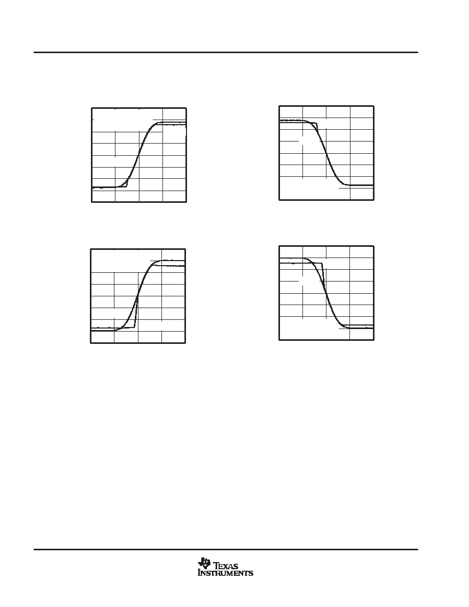
Figure 36
3
20
15
10
5
0
5
10
15
20
01
2
3
4
2
1
0
1
2
3
4
Time
s
Output
V
oltage
V
RISING EDGE OVERDRIVE RECOVERY
Input
V
oltage
V
Gain = 5,
VIN = 5.57 VPP,
Recovery Time = 340 ns
Input
Output
Figure 37
3
20
15
10
5
0
5
10
15
20
01
2
3
4
2
1
0
1
2
3
4
Time
s
Output
V
oltage
V
FALLING EDGE OVERDRIVE RECOVERY
Input
V
oltage
V
Gain = 5,
VIN = 5.57 VPP,
Recovery Time = 320 ns
Input
Output
Figure 38
3
20
15
10
5
0
5
10
15
20
01
2
3
4
2
1
0
1
2
3
4
Time
s
Output
V
oltage
V
FALLING EDGE OVERDRIVE RECOVERY
Input
V
oltage
V
Gain = 5,
VIN = 6 VPP,
Recovery Time = 540 ns
Input
Output
Figure 39
3
20
15
10
5
0
5
10
15
20
01
23
4
2
1
0
1
2
3
4
Time
s
Output
V
oltage
V
RISING EDGE OVERDRIVE RECOVERY
Input
V
oltage
V
Gain = 5,
VIN = 6 VPP,
Recovery Time = 680 ns
Input
Output
high frequency continuous wave amplification
When presented with high frequency sinusoids in low-gain configurations (G < 5), the THS4601 experiences
a relatively large differential input voltage between the two input terminals of the amplifier. As this differential
input voltage increases, the internal slew-boosting circuitry can cause some transistors in the signal path to
enter the cutoff region of operation. As the derivative of the signal changes signs, these transistors suffer from
a short recovery time period, generating appreciable levels of distortion. This behavior is depicted in the graph
Harmonic Distortion vs Frequency. At 2 MHz with a 2 VPP output signal, the distortion rises significantly. For most
high-gain configurations including transimpedance applications, this phenomena is not problematic.
slew rate performance with varying input step amplitude and rise/fall time
Some FET input amplifiers exhibit the peculiar behavior of having a larger slew rate when presented with smaller
input voltage steps and slower edge rates due to a change in bias conditions in the input stage of the amplifier
under these circumstances. This phenomena is most commonly seen when FET input amplifiers are used as
voltage followers. As this behavior is typically undesirable, the THS4601 has been designed to avoid these
issues. Larger amplitudes lead to higher slew rates, as would be anticipated, and fast edges do not degrade
the slew rate of the device.
相關PDF資料 |
PDF描述 |
|---|---|
| THS4601IDDAG3 | 1 CHANNEL, VIDEO AMPLIFIER, PDSO8 |
| THS4601IDDARG3 | 1 CHANNEL, VIDEO AMPLIFIER, PDSO8 |
| THS4601IDG4 | 1 CHANNEL, VIDEO AMPLIFIER, PDSO8 |
| THS4601CDDAR | 1 CHANNEL, VIDEO AMPLIFIER, PDSO8 |
| THS4601CDDA | 1 CHANNEL, VIDEO AMPLIFIER, PDSO8 |
相關代理商/技術參數 |
參數描述 |
|---|---|
| THS4601EVM | 功能描述:放大器 IC 開發工具 THS4601 Eval Mod RoHS:否 制造商:International Rectifier 產品:Demonstration Boards 類型:Power Amplifiers 工具用于評估:IR4302 工作電源電壓:13 V to 23 V |
| THS4601ID | 功能描述:高速運算放大器 Wideband FET-Input Op Amp RoHS:否 制造商:Texas Instruments 通道數量:1 電壓增益 dB:116 dB 輸入補償電壓:0.5 mV 轉換速度:55 V/us 工作電源電壓:36 V 電源電流:7.5 mA 最大工作溫度:+ 85 C 安裝風格:SMD/SMT 封裝 / 箱體:SOIC-8 封裝:Tube |
| THS4601IDDA | 功能描述:高速運算放大器 Wideband FET In RoHS:否 制造商:Texas Instruments 通道數量:1 電壓增益 dB:116 dB 輸入補償電壓:0.5 mV 轉換速度:55 V/us 工作電源電壓:36 V 電源電流:7.5 mA 最大工作溫度:+ 85 C 安裝風格:SMD/SMT 封裝 / 箱體:SOIC-8 封裝:Tube |
| THS4601IDDAG3 | 功能描述:高速運算放大器 Wideband FET-Input Op Amp RoHS:否 制造商:Texas Instruments 通道數量:1 電壓增益 dB:116 dB 輸入補償電壓:0.5 mV 轉換速度:55 V/us 工作電源電壓:36 V 電源電流:7.5 mA 最大工作溫度:+ 85 C 安裝風格:SMD/SMT 封裝 / 箱體:SOIC-8 封裝:Tube |
| THS4601IDDAR | 功能描述:高速運算放大器 Wideband FET-Input Op Amp RoHS:否 制造商:Texas Instruments 通道數量:1 電壓增益 dB:116 dB 輸入補償電壓:0.5 mV 轉換速度:55 V/us 工作電源電壓:36 V 電源電流:7.5 mA 最大工作溫度:+ 85 C 安裝風格:SMD/SMT 封裝 / 箱體:SOIC-8 封裝:Tube |
發布緊急采購,3分鐘左右您將得到回復。