- 您現在的位置:買賣IC網 > PDF目錄98252 > TLV2553IPWRG4 (TEXAS INSTRUMENTS INC) 11-CH 12-BIT SUCCESSIVE APPROXIMATION ADC, SERIAL ACCESS, PDSO20 PDF資料下載
參數資料
| 型號: | TLV2553IPWRG4 |
| 廠商: | TEXAS INSTRUMENTS INC |
| 元件分類: | ADC |
| 英文描述: | 11-CH 12-BIT SUCCESSIVE APPROXIMATION ADC, SERIAL ACCESS, PDSO20 |
| 封裝: | GREEN, PLASTIC, TSSOP-20 |
| 文件頁數: | 24/29頁 |
| 文件大小: | 603K |
| 代理商: | TLV2553IPWRG4 |
第1頁第2頁第3頁第4頁第5頁第6頁第7頁第8頁第9頁第10頁第11頁第12頁第13頁第14頁第15頁第16頁第17頁第18頁第19頁第20頁第21頁第22頁第23頁當前第24頁第25頁第26頁第27頁第28頁第29頁
TLV2553
SLAS354B – SEPTEMBER 2001 – REVISED SEPTEMBER 2002
4
www.ti.com
absolute maximum ratings over operating free-air temperature range (unless otherwise noted)
Supply voltage range, VCC (see Note 1)
– 0.5 V to 6.5 V
. . . . . . . . . . . . . . . . . . . . . . . . . . . . . . . . . . . . . . . . . . . . . . . . . . .
Input voltage range, VI (any input)
– 0.3 V to VCC + 0.3 V
. . . . . . . . . . . . . . . . . . . . . . . . . . . . . . . . . . . . . . . . . . . . . . . . .
Output voltage range, VO
– 0.3 V to VCC + 0.3 V
. . . . . . . . . . . . . . . . . . . . . . . . . . . . . . . . . . . . . . . . . . . . . . . . . . . . . . . .
Positive reference voltage, Vref+
–0.3 V to VCC + 0.3 V
. . . . . . . . . . . . . . . . . . . . . . . . . . . . . . . . . . . . . . . . . . . . . . . . . . .
Negative reference voltage, Vref–
–0.3 V to VCC +0.3 V
. . . . . . . . . . . . . . . . . . . . . . . . . . . . . . . . . . . . . . . . . . . . . . . . . .
Peak input current, II (any input)
±20 mA
. . . . . . . . . . . . . . . . . . . . . . . . . . . . . . . . . . . . . . . . . . . . . . . . . . . . . . . . . . . . . . . .
Peak total input current (all inputs)
±30 mA
. . . . . . . . . . . . . . . . . . . . . . . . . . . . . . . . . . . . . . . . . . . . . . . . . . . . . . . . . . . . . .
Operating virtual junction temperature range, TJ
–40
°C to 150°C
. . . . . . . . . . . . . . . . . . . . . . . . . . . . . . . . . . . . . . . . . . .
Operating free-air temperature range, TA: I
–40
°C to 85°C
. . . . . . . . . . . . . . . . . . . . . . . . . . . . . . . . . . . . . . . . . . . . . . . .
Storage temperature range, Tstg
– 65
°C to 150°C
. . . . . . . . . . . . . . . . . . . . . . . . . . . . . . . . . . . . . . . . . . . . . . . . . . . . . . . .
Lead temperature 1,6 mm (1/16 inch) from the case for 10 seconds
260
°C
. . . . . . . . . . . . . . . . . . . . . . . . . . . . . . . . . .
Stresses beyond those listed under “absolute maximum ratings” may cause permanent damage to the device. These are stress ratings only, and
functional operation of the device at these or any other conditions beyond those indicated under “recommended operating conditions” is not
implied. Exposure to absolute-maximum-rated conditions for extended periods may affect device reliability.
NOTE 1: All voltage values are with respect to the GND terminal with REF – and GND wired together (unless otherwise noted).
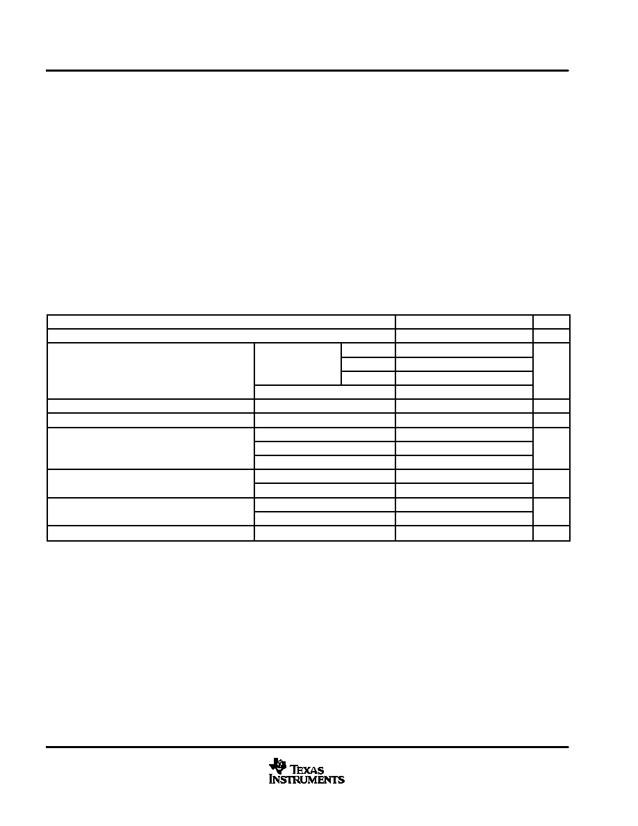
recommended operating conditions
PARAMETERS
MIN
NOM
MAX
UNIT
Supply voltage, VCC
2.7
5.5
V
16-bit I/O
0.01
15
I/O CLOCK frequency
VCC = 4.5 V to 5.5 V
12-bit I/O
0.01
15
MHz
I/O CLOCK frequency
8-bit I/O
0.01
15
MHz
VCC = 2.7 V to 3.6 V
0.01
10
Tolerable clock jitter, I/O CLOCK
VCC = 4.5 V to 5.5 V
0.38
ns
Aperature jitter
VCC = 4.5 V to 5.5 V
100
ps
VCC = 4.5 V to 5.5 V
0
(REF+) – (REF–)
Analog input voltage (see Note 2)
VCC = 3.0 V to 3.6 V
0
(REF+ ) –(REF–)
V
VCC = 2.7 V to 3.0 V
0
(REF+) –(REF–)
High level control input voltage VIH
VCC = 4.5 V to 5.5 V
2.0
V
High-level control input voltage, VIH
VCC = 2.7 V to 3.6 V
2.1
V
Low level control input voltage VIL
VCC = 4.5 V to 5.5 V
0.8
V
Low-level control input voltage, VIL
VCC = 2.7 V to 3.6 V
0.6
V
Operating free-air temperature, TA
TLV2553I
–40
85
°C
NOTE 2: Analog input voltages greater than the voltage applied to REF+ convert as all ones (111111111111), while input voltages less than the
voltage applied to REF– convert as all zeros (000000000000).
相關PDF資料 |
PDF描述 |
|---|---|
| TLV2553IDW | 11-CH 12-BIT SUCCESSIVE APPROXIMATION ADC, SERIAL ACCESS, PDSO20 |
| TLV2553IPWG4 | 11-CH 12-BIT SUCCESSIVE APPROXIMATION ADC, SERIAL ACCESS, PDSO20 |
| TLV2553IPW | 11-CH 12-BIT SUCCESSIVE APPROXIMATION ADC, SERIAL ACCESS, PDSO20 |
| TLV2553IDWR | 11-CH 12-BIT SUCCESSIVE APPROXIMATION ADC, SERIAL ACCESS, PDSO20 |
| TLV2553IDWRQ1 | 11-CH 12-BIT SUCCESSIVE APPROXIMATION ADC, SERIAL ACCESS, PDSO20 |
相關代理商/技術參數 |
參數描述 |
|---|---|
| TLV2553IPWRQ1 | 功能描述:12 Bit Analog to Digital Converter 11 Input 1 SAR 20-TSSOP 制造商:texas instruments 系列:- 包裝:剪切帶(CT) 零件狀態:有效 位數:12 采樣率(每秒):200k 輸入數:11 輸入類型:單端 數據接口:SPI 配置:MUX-S/H-ADC 無線電 - S/H:ADC:1:1 A/D 轉換器數:1 架構:SAR 參考類型:外部 電壓 - 電源,模擬:2.7 V ~ 5.5 V 電壓 - 電源,數字:2.7 V ~ 5.5 V 特性:- 工作溫度:-40°C ~ 85°C 封裝/外殼:20-TSSOP(0.173",4.40mm 寬) 供應商器件封裝:20-TSSOP 標準包裝:1 |
| TLV2556EVM | 功能描述:數據轉換 IC 開發工具 TLV2556 Eval Mod RoHS:否 制造商:Texas Instruments 產品:Demonstration Kits 類型:ADC 工具用于評估:ADS130E08 接口類型:SPI 工作電源電壓:- 6 V to + 6 V |
| TLV2556IDW | 功能描述:模數轉換器 - ADC 12-Bit 200 KSPS 11 Ch Lo-Pwr RoHS:否 制造商:Texas Instruments 通道數量:2 結構:Sigma-Delta 轉換速率:125 SPs to 8 KSPs 分辨率:24 bit 輸入類型:Differential 信噪比:107 dB 接口類型:SPI 工作電源電壓:1.7 V to 3.6 V, 2.7 V to 5.25 V 最大工作溫度:+ 85 C 安裝風格:SMD/SMT 封裝 / 箱體:VQFN-32 |
| TLV2556IDWG4 | 功能描述:模數轉換器 - ADC 12-Bit 200 KSPS 11 Ch Lo-Pwr RoHS:否 制造商:Texas Instruments 通道數量:2 結構:Sigma-Delta 轉換速率:125 SPs to 8 KSPs 分辨率:24 bit 輸入類型:Differential 信噪比:107 dB 接口類型:SPI 工作電源電壓:1.7 V to 3.6 V, 2.7 V to 5.25 V 最大工作溫度:+ 85 C 安裝風格:SMD/SMT 封裝 / 箱體:VQFN-32 |
| TLV2556IDWR | 功能描述:模數轉換器 - ADC 12-Bit 200 KSPS 11 Ch Lo-Pwr RoHS:否 制造商:Texas Instruments 通道數量:2 結構:Sigma-Delta 轉換速率:125 SPs to 8 KSPs 分辨率:24 bit 輸入類型:Differential 信噪比:107 dB 接口類型:SPI 工作電源電壓:1.7 V to 3.6 V, 2.7 V to 5.25 V 最大工作溫度:+ 85 C 安裝風格:SMD/SMT 封裝 / 箱體:VQFN-32 |
發布緊急采購,3分鐘左右您將得到回復。