- 您現(xiàn)在的位置:買賣IC網(wǎng) > PDF目錄98252 > TLV320AIC10IGQER (TEXAS INSTRUMENTS INC) SPECIALTY CONSUMER CIRCUIT, PBGA80 PDF資料下載
參數(shù)資料
| 型號: | TLV320AIC10IGQER |
| 廠商: | TEXAS INSTRUMENTS INC |
| 元件分類: | 消費家電 |
| 英文描述: | SPECIALTY CONSUMER CIRCUIT, PBGA80 |
| 封裝: | MICRO, PLASTIC, BGA-80 |
| 文件頁數(shù): | 17/57頁 |
| 文件大小: | 454K |
| 代理商: | TLV320AIC10IGQER |
第1頁第2頁第3頁第4頁第5頁第6頁第7頁第8頁第9頁第10頁第11頁第12頁第13頁第14頁第15頁第16頁當前第17頁第18頁第19頁第20頁第21頁第22頁第23頁第24頁第25頁第26頁第27頁第28頁第29頁第30頁第31頁第32頁第33頁第34頁第35頁第36頁第37頁第38頁第39頁第40頁第41頁第42頁第43頁第44頁第45頁第46頁第47頁第48頁第49頁第50頁第51頁第52頁第53頁第54頁第55頁第56頁第57頁
2–10
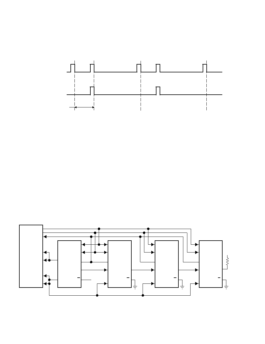
2.7.4
Frame-Sync (FS) Function—Slave Mode
The slave mode is selected by connecting pin M/S to LO. The frame-sync timing is generated externally by the master,
as shown in Figure 2–13 (that is, FSD) and is applied to FS of the slave to control the ADC and DAC timing.
MP
32 SCLKs
FSD (Master)
to FS (Slave)
FS
(Master to DSP)
SP
MS
SS
MP
NOTE: MP: master primary (master-device data is transferred during this period, the DOUT of the slave device is in high-impedance state).
SP: slave primary (slave device data is transferred during this period, the DOUT of master device is in high-impedance state).
MS: master secondary (master device control register information is transferred during this period, the DOUT of slave device is in high-
impedance state).
SS: slave secondary (slave device control register information is transferred during this period, the DOUT of master device is in high-
impedance state).
Figure 2–13. Master Device’s FS Output to DSP and FSD Output to the Slave
2.7.5
Frame-Sync Delayed (FSD) Function, Cascade Mode
In cascade mode, the DSP must be able to identify the master and slaves according to the register map shown in
Appendix A. Each device in the cascade contains a 3-bit cascade register (D15-D13 in the register address) that has
been programmed by the ACD (automatic cascade detection) with an address value equal to its position in the
cascade during the device’s power-up initialization (see Appendix A). The device address of the master is always
equal to the number of slaves in the cascade. For example, in Figure 2–14, D15-D13 of the master is 011, as shown
in row 4 of Table A-1 (Appendix A). The DSP receives all frame-sync pulses from the master though the masters FS.
The master FSD is output to the first slave, and the first slave FSD is output to the second slave device, and so on.
Figure 2–14 shows the cascade of 4 TLV320AIC10s in which the closest one to the DSP is the master, and the rest
are slaves. The FSD output of each device is input to the FS terminal of the succeeding device. Figure 2–15 shows
the FSD timing sequence in the cascade.
MCLK
DIN
DOUT
FS
SCLK
MCLK
DIN
DOUT
FS
SCLK
MCLK
DIN
DOUT
FS
SCLK
Slave 2
Slave 1
Slave 0
Master
MCLK
DIN
DOUT
FSD
SCLK
FSD
FS
CLKOUT
DX
DR
FSX
FSR
CLKX
CLKR
TMS320C54XX
DVDD
FSD
M/S
(or Master Clock Source)
DVDD
1 k
Figure 2–14. Cascade Mode Connection (to DSP Interface)
相關PDF資料 |
PDF描述 |
|---|---|
| TLV320AIC11C | SPECIALTY CONSUMER CIRCUIT, PQFP48 |
| TLV320AIC11I | SPECIALTY CONSUMER CIRCUIT, PQFP48 |
| TLV320AIC11CPFB | SPECIALTY CONSUMER CIRCUIT, PQFP48 |
| TLV320AIC11IPFB | SPECIALTY CONSUMER CIRCUIT, PQFP48 |
| TLV320AIC11CPFBG4 | SPECIALTY CONSUMER CIRCUIT, PQFP48 |
相關代理商/技術參數(shù) |
參數(shù)描述 |
|---|---|
| TLV320AIC10IPFB | 功能描述:接口—CODEC 16-Bit 22-KSPS DSP Codec RoHS:否 制造商:Texas Instruments 類型: 分辨率: 轉換速率:48 kSPs 接口類型:I2C ADC 數(shù)量:2 DAC 數(shù)量:4 工作電源電壓:1.8 V, 2.1 V, 2.3 V to 5.5 V 最大工作溫度:+ 85 C 安裝風格:SMD/SMT 封裝 / 箱體:DSBGA-81 封裝:Reel |
| TLV320AIC10IPFBG4 | 功能描述:接口—CODEC 18-Bit Regstr Bus Trncvr W/3-St Otpt RoHS:否 制造商:Texas Instruments 類型: 分辨率: 轉換速率:48 kSPs 接口類型:I2C ADC 數(shù)量:2 DAC 數(shù)量:4 工作電源電壓:1.8 V, 2.1 V, 2.3 V to 5.5 V 最大工作溫度:+ 85 C 安裝風格:SMD/SMT 封裝 / 箱體:DSBGA-81 封裝:Reel |
| TLV320AIC10PFB | 制造商:TI 制造商全稱:Texas Instruments 功能描述:General-Purpose 3V to 5.5V 16-bit 22-KSPS DSP CODEC |
| TLV320AIC11 | 制造商:TI 制造商全稱:Texas Instruments 功能描述:General-Purpose Low-Voltage 1.1V to 3.6V/0 16-bit 22-KSPS DSP CODEC |
| TLV320AIC1103 | 制造商:TI 制造商全稱:Texas Instruments 功能描述:PCM CODEC |
發(fā)布緊急采購,3分鐘左右您將得到回復。