- 您現在的位置:買賣IC網 > PDF目錄98252 > TLV320AIC22PT (TEXAS INSTRUMENTS INC) SPECIALTY CONSUMER CIRCUIT, PQFP48 PDF資料下載
參數資料
| 型號: | TLV320AIC22PT |
| 廠商: | TEXAS INSTRUMENTS INC |
| 元件分類: | 消費家電 |
| 英文描述: | SPECIALTY CONSUMER CIRCUIT, PQFP48 |
| 封裝: | ROHS COMPLIANT, PLASTIC, LQFP-48 |
| 文件頁數: | 34/55頁 |
| 文件大小: | 782K |
| 代理商: | TLV320AIC22PT |
第1頁第2頁第3頁第4頁第5頁第6頁第7頁第8頁第9頁第10頁第11頁第12頁第13頁第14頁第15頁第16頁第17頁第18頁第19頁第20頁第21頁第22頁第23頁第24頁第25頁第26頁第27頁第28頁第29頁第30頁第31頁第32頁第33頁當前第34頁第35頁第36頁第37頁第38頁第39頁第40頁第41頁第42頁第43頁第44頁第45頁第46頁第47頁第48頁第49頁第50頁第51頁第52頁第53頁第54頁第55頁
TLV320AIC22
DUAL VOIP CODEC
SLAS281B – JULY 2000 – REVISED JUNE 2002
4
POST OFFICE BOX 655303
DALLAS, TEXAS 75265
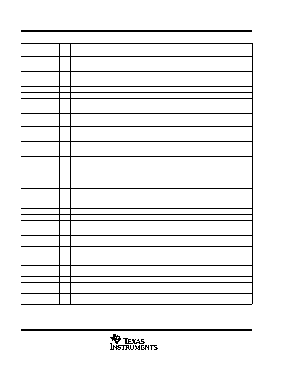
Terminal Functions
TERMINAL
I/O
DESCRIPTION
NAME
NO.
I/O
DESCRIPTION
AD1
12
I
In I2C mode, AD1 is used with AD0 to form the lower two bits of the 7-bit I2C chip address. The upper five bits are
fixed at 11100. AD1 also is used in conjunction with AD0 to assign the two time slots for the codec in serial-port
mode. AD1 is the MSB.
AD0
13
I
In I2C mode, AD0 is used with AD1 to form the lower two bits of the 7-bit I2C chip address. The upper five bits are
fixed at 11100. AD0 also is used in conjunction with AD1 to assign the two time slots for the codec in serial-port
mode. AD0 is the LSB.
AVDD1
33
I
Analog power supply. Connect to AVDD2. See Note 3
AVDD2
5
I
Analog power supply. Connect to AVDD1. See Note 3
AVDD3
27
I
Analog power supply for 8-
speaker driver. This pin can be connected to AVDD1andAVDD2.Becausethissignal
requires large amounts of current, it is recommended that a separate PCB trace be run to this pin and connected to
the main supply at the power-supply connection to the PC board. See Note 3
AVSS1
32
I
Analog ground. Connect to AVSS2. See Note 3
AVSS2
6
I
Analog ground. Connect to AVSS1. See Note 3
AVSS3
25, 29
I
Analog ground for 8-
speaker driver. These pins can be connected to AVSS1 and AVSS2. Because this signal
requires large amounts of current, it is recommended that a separate PCB trace be run to this pin and connected to
the main supply at the power-supply connection to the PC board. See Note 3
BCLK
20
I/O
Bit clock. BCLK clocks serial data into DIN and out of DOUT. When configured as an output (master mode), BCLK
is generated internally by multiplying the frame-sync signal frequency by 256. When configured as an input (slave
mode), BCLK is an input and must be synchronous with the master clock and frame sync.
CIINM
30
I
CallerID amplifier analog inverting input
CIINP
31
I
CallerID amplifier analog noninverting input
DIN
18
I
Data input. DIN receives the DAC input data and register data from the external digital signal processor (DSP) or
controller and is synchronized to BCLK. Data is latched on the falling edge of BCLK in the two time slots that are
specified by the AD1 and AD0 bits. Codec 1 receives data in the first assigned time slot, followed by codec 2
receiving data in the second assigned time slot.
DOUT
17
O
Data output. DOUT transmits the ADC output bits and the register data. It is synchronized to BCLK. Data is
transmitted on the rising edge of BCLK in the two time slots that are specified by the AD1 and AD0 bits. DOUT is at
high impedance during time slots not assigned to the codec. Codec 1 transmits data in the first assigned time slot,
followed by codec 2 in the second assigned time slot.
DVDD
15
I
Digital power supply. See Note 3
DVSS
16
I
Digital ground. See Note 3
FILT1
43
O
Reference filter node. FILT1 and FILT2 provide decoupling of the reference voltage. This reference is 2.25 V. The
optimal capacitor value is 0.1
F (ceramic) and is connected between FILT1 and FILT2. FILT1 should not be used
as a voltage source.
FILT2
42
O
Reference filter node. FILT1 and FILT2 provide decoupling of the reference voltage. This reference is 0 V. The
optimal capacitor value is 0.1
F (ceramic) and is connected between FILT1 and FILT2.
FSYNC
19
I/O
Frame sync. FSYNC indicates the beginning of a frame and the start of time slot 0. When FSYNC is sampled high
on the rising edge of BCLK, the codec receives or transmits data in its specified time slot (specified by AD0 and
AD1) in the frame. FSYNC is generated by the master device (output) and is an input to the slave devices. Codec 1
communicates in the first assigned time slot, followed by codec 2 communicating in the second assigned time slot.
HDINM
1
I
Headset amplifier analog inverting input. A connection between HDIN and HDOUT occurs, with selected echo
gain, unless the echo gain is muted. See register 14
HDINP
2
I
Headset amplifier analog noninverting input
HDOUTM
3
O
Inverting headset output. The HDOUTM pin, together with the HDOUTP pin, forms the differential output. With
HDOUTP, a 150-
load can be driven, differentially. HDOUTM also can be used alone for single-ended operation.
HDOUTP
4
O
Noninverting headset output. HDOUTP can be used alone for single-ended operation. With HDOUTM, a 150-
load can be driven, differentially.
NOTE 3: This device has separate analog and digital power and ground pins. For best operation and results, the PC board design should utilize
separate analog and digital power supplies as well as separate analog and digital ground planes. Mixed-signal design practices should
be used.
相關PDF資料 |
PDF描述 |
|---|---|
| TLV320AIC22PTR | SPECIALTY CONSUMER CIRCUIT, PQFP48 |
| TLV320AIC23BGQE | SPECIALTY CONSUMER CIRCUIT, PBGA80 |
| TLV320AIC23BIGQE | SPECIALTY CONSUMER CIRCUIT, PBGA80 |
| TLV320AIC23BIPW | SPECIALTY CONSUMER CIRCUIT, PDSO28 |
| TLV320AIC23BPW | SPECIALTY CONSUMER CIRCUIT, PDSO28 |
相關代理商/技術參數 |
參數描述 |
|---|---|
| TLV320AIC22PTR | 功能描述:接口—CODEC DUAL VOIP CODEC RoHS:否 制造商:Texas Instruments 類型: 分辨率: 轉換速率:48 kSPs 接口類型:I2C ADC 數量:2 DAC 數量:4 工作電源電壓:1.8 V, 2.1 V, 2.3 V to 5.5 V 最大工作溫度:+ 85 C 安裝風格:SMD/SMT 封裝 / 箱體:DSBGA-81 封裝:Reel |
| TLV320AIC23 | 制造商:TI 制造商全稱:Texas Instruments 功能描述:STereo Audio CODEC, 8- to 96kHz, With Integrated Headphone Amplifier |
| TLV320AIC23_06 | 制造商:TI 制造商全稱:Texas Instruments 功能描述:Stereo Audio CODEC, 8-to 96-kHz, With Integrated Headphone Amplifier |
| TLV320AIC23B | 制造商:TI 制造商全稱:Texas Instruments 功能描述:Stereo Audio CODEC, 8-to 96-kHz, With Integrated Headphone Amplifier |
| TLV320AIC23B_06 | 制造商:TI 制造商全稱:Texas Instruments 功能描述:Stereo Audio CODEC, 8-to 96-kHz, With Integrated Headphone Amplifier |
發布緊急采購,3分鐘左右您將得到回復。