- 您現在的位置:買賣IC網 > PDF目錄98254 > TLV320AIC33IZQER (TEXAS INSTRUMENTS INC) SPECIALTY CONSUMER CIRCUIT, PBGA80 PDF資料下載
參數資料
| 型號: | TLV320AIC33IZQER |
| 廠商: | TEXAS INSTRUMENTS INC |
| 元件分類: | 消費家電 |
| 英文描述: | SPECIALTY CONSUMER CIRCUIT, PBGA80 |
| 封裝: | 5 X 5 MM, ROHS COMPLIANT, PLASTIC, VFBGA-80 |
| 文件頁數: | 11/93頁 |
| 文件大小: | 1427K |
| 代理商: | TLV320AIC33IZQER |
第1頁第2頁第3頁第4頁第5頁第6頁第7頁第8頁第9頁第10頁當前第11頁第12頁第13頁第14頁第15頁第16頁第17頁第18頁第19頁第20頁第21頁第22頁第23頁第24頁第25頁第26頁第27頁第28頁第29頁第30頁第31頁第32頁第33頁第34頁第35頁第36頁第37頁第38頁第39頁第40頁第41頁第42頁第43頁第44頁第45頁第46頁第47頁第48頁第49頁第50頁第51頁第52頁第53頁第54頁第55頁第56頁第57頁第58頁第59頁第60頁第61頁第62頁第63頁第64頁第65頁第66頁第67頁第68頁第69頁第70頁第71頁第72頁第73頁第74頁第75頁第76頁第77頁第78頁第79頁第80頁第81頁第82頁第83頁第84頁第85頁第86頁第87頁第88頁第89頁第90頁第91頁第92頁第93頁
RA(6)
RA(5)
RA(0)
D(7)
D(6)
D(0)
Read
/SS
SCLK
MOSI
MISO
DON’T CARE
8-Bit Register Data
7-Bit Register Address
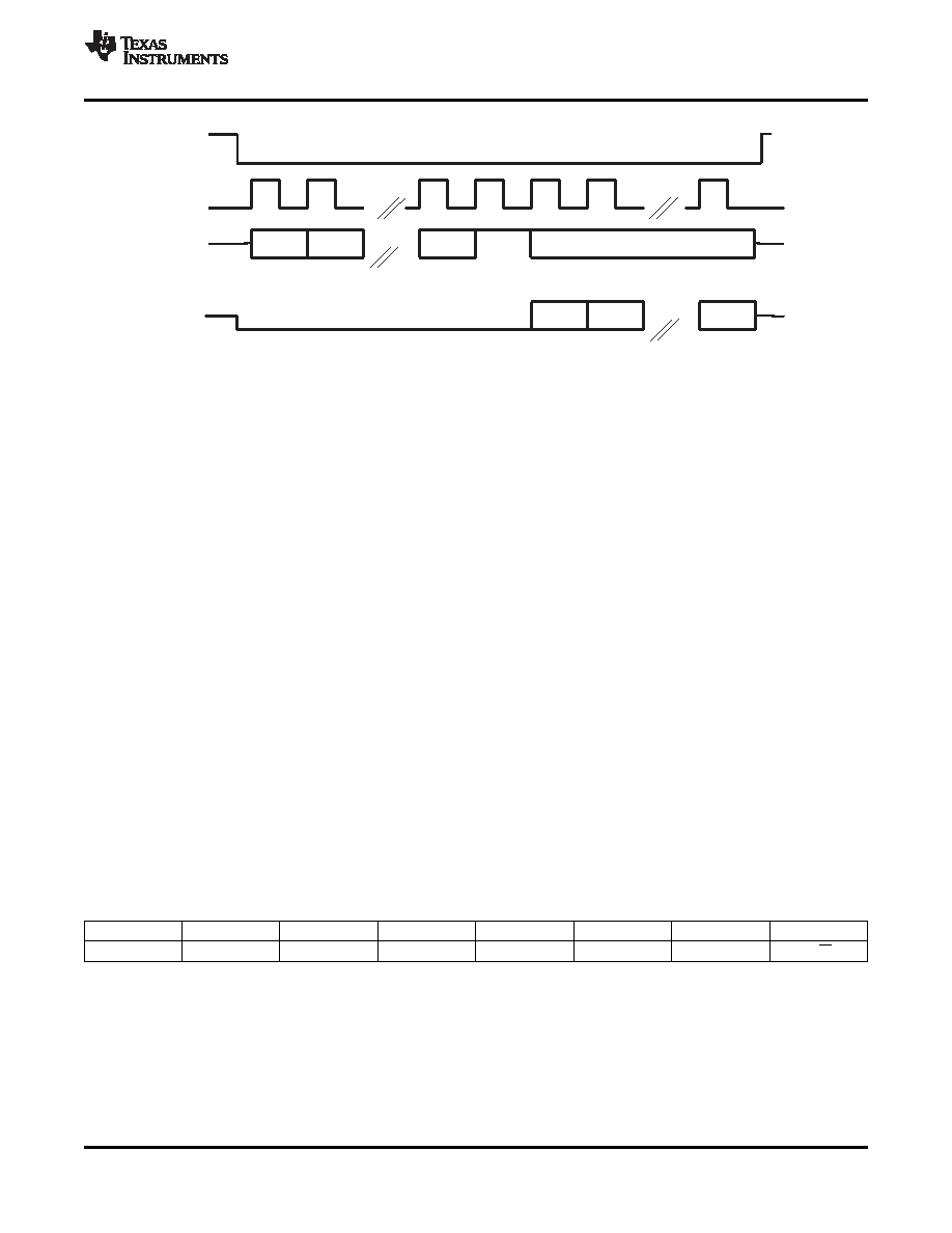
SPI COMMUNICATION PROTOCOL
www.ti.com ........................................................................................................................................... SLAS480B – JANUARY 2006 – REVISED DECEMBER 2008
Figure 16. SPI Read
In the SPI control mode, the TLV320AIC33 uses the pins MFP0=SSB, MFP1=SCLK, MFP2=MISO, MFP3=MOSI
as a standard SPI port with clock polarity setting of 0 (typical microprocessor SPI control bit CPOL = 0). The SPI
port allows full-duplex, synchronous, serial communication between a host processor (the master) and peripheral
devices (slaves). The SPI master (in this case, the host processor) generates the synchronizing clock (driven
onto SCLK) and initiates transmissions. The SPI slave devices (such as the TLV320AIC33) depend on a master
to start and synchronize transmissions.
A transmission begins when initiated by an SPI master. The byte from the SPI master begins shifting in on the
slave MOSI pin under the control of the master serial clock (driven onto SCLK). As the byte shifts in on the MOSI
pin, a byte shifts out on the MISO pin to the master shift register.
The TLV320AIC33 interface is designed so that with a clock phase bit setting of 1 (typical microprocessor SPI
control bit CPHA = 1), the master begins driving its MOSI pin and the slave begins driving its MISO pin on the
first serial clock edge. The SSB pin can remain low between transmissions; however, the TLV320AIC33 only
interprets the first 8 bits transmitted after the falling edge of SSB as a command byte, and the next 8 bits as a
data byte only if writing to a register. Reserved register bits should be written to their default values.
The TLV320AIC33 is entirely controlled by registers. Reading and writing these registers is accomplished by the
use of an 8-bit command, which is sent to the MOSI pin of the part prior to the data for that register. The
command is constructed as shown in the Command Word table. The first 7 bits specify the register address
which is being written or read, from 0 to 127 (decimal). The command word ends with an R/W bit, which specifies
the direction of data flow on the serial bus. In the case of a register write, the R/W bit should be set to 0. A
second byte of data is sent to the MOSI pin and contains the data to be written to the register.
Reading of registers is accomplished in similar fashion. The 8-bit command word sends the 7-bit register
address, followed by R/W bit = 1 to signify a register read is occurring,. The 8-bit register data is then clocked out
of the part on the MISO pin during the second 8 SCLK clocks in the frame.
Command Word
Bit 7
Bit 6
Bit 5
Bit 4
Bit 3
Bit 2
Bit 1
Bit 0
ADDR6
ADDR5
ADDR4
ADDR3
ADDR2
ADDR1
ADDR0
R/W
The register map of the TLV320AIC33 actually consists of multiple pages of registers, with each page containing
128 registers. The register at address zero on each page is used as a page-control register, and writing to this
register determines the active page for the device. All subsequent read/write operations will access the page that
is active at the time, unless a register write is performed to change the active page. Only two pages of registers
are implemented in this product, with the active page defaulting to page 0 upon device reset.
For example, at device reset, the active page defaults to page 0, and thus all register read/write operations for
addresses 1 to 127 will access registers in page 0. If registers on page 1 must be accessed, the user must write
the 8-bit sequence 0x01 to register 0, the page control register, to change the active page from page 0 to page 1.
After this write, it is recommended the user also read back the page control register, to safely ensure the change
Copyright 2006–2008, Texas Instruments Incorporated
19
Product Folder Link(s): TLV320AIC33
相關PDF資料 |
PDF描述 |
|---|---|
| TLV320AIC33IZQE | SPECIALTY CONSUMER CIRCUIT, PBGA80 |
| TLV320AIC33IRGZT | SPECIALTY CONSUMER CIRCUIT, PQCC48 |
| TLV320AIC33IRGZRG4 | SPECIALTY CONSUMER CIRCUIT, PQCC48 |
| TLV320AIC33IRGZTG4 | SPECIALTY CONSUMER CIRCUIT, PQCC48 |
| TLV320AIC33IRGZ | SPECIALTY CONSUMER CIRCUIT, PQCC48 |
相關代理商/技術參數 |
參數描述 |
|---|---|
| TLV320AIC33NIZQE | 制造商:Texas Instruments 功能描述: |
| TLV320AIC33NIZQER | 制造商:Texas Instruments 功能描述: |
| TLV320AIC33RHBRG4 | 制造商:Texas Instruments 功能描述:CODEC - Tape and Reel |
| TLV320AIC34 | 制造商:TI 制造商全稱:Texas Instruments 功能描述:FOUR-CHANNEL, LOW-POWER AUDIO CODEC FOR PORTABLE AUDIO/TELEPHONY |
| TLV320AIC34_1 | 制造商:TI 制造商全稱:Texas Instruments 功能描述:FOUR-CHANNEL, LOW-POWER AUDIO CODEC FOR PORTABLE AUDIO/TELEPHONY |
發布緊急采購,3分鐘左右您將得到回復。