- 您現在的位置:買賣IC網 > PDF目錄98255 > TLV5580IPWRG4 (TEXAS INSTRUMENTS INC) 1-CH 8-BIT PROPRIETARY METHOD ADC, PARALLEL ACCESS, PDSO28 PDF資料下載
參數資料
| 型號: | TLV5580IPWRG4 |
| 廠商: | TEXAS INSTRUMENTS INC |
| 元件分類: | ADC |
| 英文描述: | 1-CH 8-BIT PROPRIETARY METHOD ADC, PARALLEL ACCESS, PDSO28 |
| 封裝: | GREEN, PLASTIC, TSSOP-28 |
| 文件頁數: | 8/36頁 |
| 文件大小: | 478K |
| 代理商: | TLV5580IPWRG4 |
第1頁第2頁第3頁第4頁第5頁第6頁第7頁當前第8頁第9頁第10頁第11頁第12頁第13頁第14頁第15頁第16頁第17頁第18頁第19頁第20頁第21頁第22頁第23頁第24頁第25頁第26頁第27頁第28頁第29頁第30頁第31頁第32頁第33頁第34頁第35頁第36頁
TLV5580
8BIT, 80 MSPS LOW POWER A/D CONVERTER
SLAS205B DECEMBER 1998 REVISED OCTOBER 2003
www.ti.com
16
PRINCIPLE OF OPERATION
REFERENCE TERMINALS
The voltages on terminals REFBI and REFTI determine the TLV5580’s input range. Since the device has an
internal voltage reference generator with outputs available on REFBO respectively REFTO, corresponding
terminals can be directly connected externally to provide a contained ADC solution. Especially at higher
sampling rates, it is advantageous to have a wider analog input range. The wider analog input range is
achievable by using external voltage references (e.g., at AVDD = 3.3 V, the full scale range can be extended
from 1 Vpp (internal reference) to 1.3 Vpp (external reference) as shown in Table 1). These voltages should
not be derived via a voltage divider from a power supply source. Instead, use a bandgap-derived voltage
reference to derive both references via an op amp circuit. Refer to the schematic of the TLV5580 evaluation
module for an example circuit.
When using external references, the full-scale ADC input range and its dc position can be adjusted. The
full-scale ADC range is always equal to VREFT – VREFB. The maximum full-scale range is dependent on AVDD
as shown in the specification section. In addition to the limitation on their difference, VREFT and VREFB each
also have limits on their useful range. These limits are also dependent on AVDD.
Table 3 summarizes these limits for 3 cases.
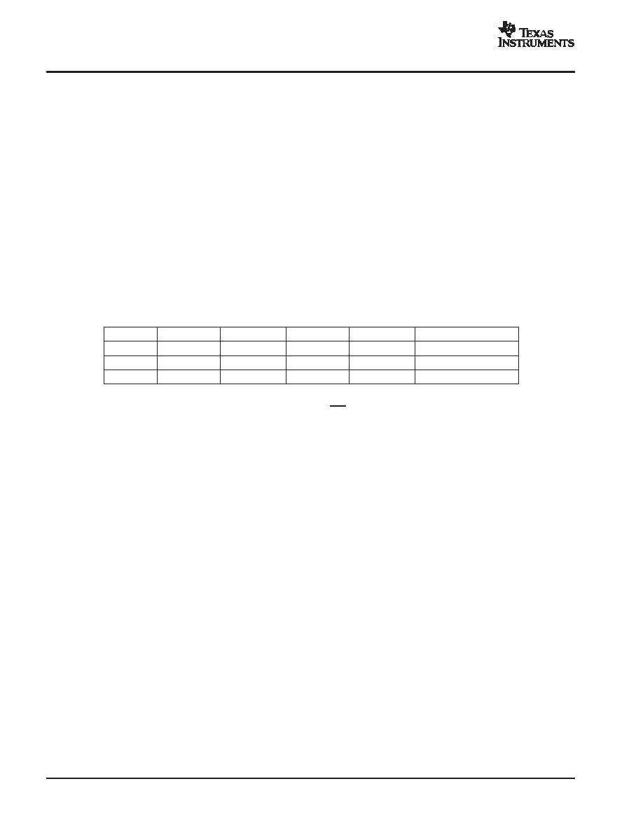
Table 1. Recommended Operating Modes
AVDD
VREFB(min)
VREFB(max)
VREFT(min)
VREFT(max)
[VREFTVREFB]max
3 V
0.8 V
1.2 V
1.8 V
2.2 V
1 V
3.3 V
0.8 V
1.2 V
2.1 V
2.5 V
1.3 V
3.6 V
0.8 V
1.2 V
2.4 V
2.8 V
1.6 V
DIGITAL INPUTS
The digital inputs are CLK, STDBY, PWDN_REF, and OE. All these signals, except CLK, have an internal
pull-down resistor to connect to digital ground. This provides a default active operation mode using internal
references when left unconnected.
The CLK signal at high frequencies should be considered as an analog input. Overshoot/undershoot should
be minimized by proper termination of the signal close to the TLV5580. An important cause of performance
degradation for a high-speed ADC is clock jitter. Clock jitter causes uncertainty in the sampling instant of the
ADC, in addition to the inherent uncertainty on the sampling instant caused by the part itself, as specified by
its aperture jitter. There is a theoretical relationship between the frequency (f) and resolution (2N) of a signal
that needs to be sampled and the maximum amount of aperture error dtmax that is tolerable. The following
formula shows the relation:
dtmax + 1 B p f2
N
)1
As an example, for an 8bit converter with a 15-MHz input, the jitter needs to be kept <41 pF in order not to
have changes in the LSB of the ADC output due to the total aperture error.
相關PDF資料 |
PDF描述 |
|---|---|
| TLV5580IDWR | 1-CH 8-BIT PROPRIETARY METHOD ADC, PARALLEL ACCESS, PDSO28 |
| TLV5580IPW | 1-CH 8-BIT PROPRIETARY METHOD ADC, PARALLEL ACCESS, PDSO28 |
| TLV5580IPWR | 1-CH 8-BIT PROPRIETARY METHOD ADC, PARALLEL ACCESS, PDSO28 |
| TLV5580IDWG4 | 1-CH 8-BIT PROPRIETARY METHOD ADC, PARALLEL ACCESS, PDSO28 |
| TLV5580CDWG4 | 1-CH 8-BIT PROPRIETARY METHOD ADC, PARALLEL ACCESS, PDSO28 |
相關代理商/技術參數 |
參數描述 |
|---|---|
| TLV5580PW | 制造商:TI 制造商全稱:Texas Instruments 功能描述:8-BIT, 80 MSPS LOW-POWER A/D CONVERTER |
| TLV5590 | 制造商:TI 制造商全稱:Texas Instruments 功能描述:2-BIT ANALOG-TO-DIGITAL CONVERTER FOR FLEX |
| TLV5590ED | 制造商:Rochester Electronics LLC 功能描述:- Bulk |
| TLV5590EDR | 制造商:Rochester Electronics LLC 功能描述:- Bulk |
| TLV5590EPWR | 制造商:Texas Instruments 功能描述: |
發布緊急采購,3分鐘左右您將得到回復。