- 您現在的位置:買賣IC網 > PDF目錄98258 > TLV5614IYZR (TEXAS INSTRUMENTS INC) SERIAL INPUT LOADING, 9 us SETTLING TIME, 12-BIT DAC, UUC16 PDF資料下載
參數資料
| 型號: | TLV5614IYZR |
| 廠商: | TEXAS INSTRUMENTS INC |
| 元件分類: | DAC |
| 英文描述: | SERIAL INPUT LOADING, 9 us SETTLING TIME, 12-BIT DAC, UUC16 |
| 封裝: | GREEN, DIE-16 |
| 文件頁數: | 19/25頁 |
| 文件大小: | 500K |
| 代理商: | TLV5614IYZR |
www.ti.com
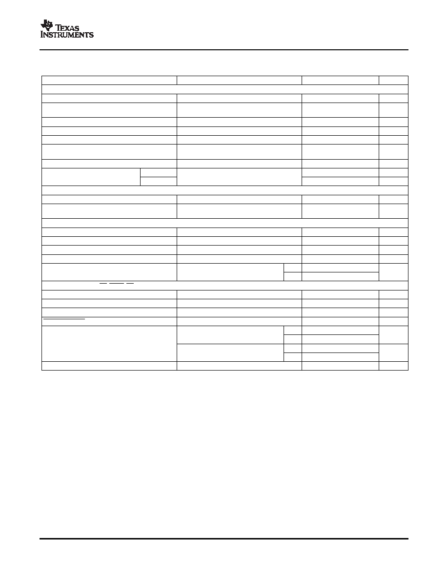
ELECTRICAL CHARACTERISTICS
SBAS401 – DECEMBER 2006
Over operating free-air temperature range, supply voltages, and reference voltages (unless otherwise noted).
PARAMETER
TEST CONDITIONS
MIN
TYP
MAX
UNIT
STATIC DAC SPECIFICATIONS
Resolution
12
bits
Integral nonlinearity (INL), end point
adjusted
See(1)
±1.5
±4
LSB
Differential nonlinearity (DNL)
See(2)
±0.5
±1
LSB
EZS
Zero-scale error (offset error at zero scale)
See(3)
±12
mV
Zero-scale error temperature coefficient
See(4)
10
ppm/
°C
% of FS
EG
Gain error
See(5)
±0.6
voltage
Gain error temperature coefficient
See(6)
10
ppm/
°C
Zero scale
–80
dB
PSRR
Power supply rejection ratio
See(7)(8)
Full scale
–80
dB
INDIVIDUAL DAC OUTPUT SPECIFICATIONS
VO
Voltage output range
RL = 10k
0
AVDD – 0.4
V
% of FS
Output load regulation accuracy
RL = 2k vs 10k
0.1
0.25
voltage
REFERENCE INPUTS (REFINAB, REFINCD)
VI
Input voltage range
See(9)
0
AVDD – 1.5
V
RI
Input resistance
10
M
CI
Input capacitance
5
pF
Reference feedthrough
REFIN = 1VPP at 1kHz + 1.024VDC (see(10))
–75
dB
Slow
0.5
Reference input bandwidth
REFIN = 0.2VPP + 1.024VDC large signal
MHz
Fast
1
DIGITAL INPUTS (DIN, CS, LDAC, PD)
IIH
High-level digital input current
VI = VDD
±1
A
IIL
Low-level digital input current
VI = 0V
±1
A
CI
Input capacitance
3
pF
POWER SUPPLY
Slow
1.6
2.4
5V supply, no load, clock running.
mA
All inputs 0V or VDD
Fast
3.8
5.6
IDD
Power supply current
Slow
1.2
1.8
3V supply, no load, clock running.
mA
All inputs 0V or DVDD
Fast
3.2
4.8
Power down supply current (see Figure 12)
10
nA
(1)
The relative accuracy or integral nonlinearity (INL), sometimes referred to as linearity error, is the maximum deviation of the output from
the line between zero and full-scale excluding the effects of zero code and full-scale errors.
(2)
The differential nonlinearity (DNL), sometimes referred to as differential error, is the difference between the measured and ideal 1 LSB
amplitude change of any two adjacent codes. Monotonic means the output voltage changes in the same direction (or remains constant)
as a change in the digital input code.
(3)
Zero-scale error is the deviation from zero voltage output when the digital input code is zero.
(4)
Zero-scale error temperature coefficient is given by: EZS TC = [EZS (TMAX) – EZS (TMIN)]/VREF × 106/(TMAX – TMIN).
(5)
Gain error is the deviation from the ideal output (2VREF – 1 LSB) with an output load of 10 k excluding the effects of the zero error.
(6)
Gain temperature coefficient is given by: EG TC = [EG(TMAX) – EG (TMIN)]/VREF × 106/(TMAX – TMIN).
(7)
Zero-scale error rejection ratio (EZS–RR) is measured by varying the AVDD from 5V ± 0.5V and 3V ± 0.3VDC, and measuring the
proportion of this signal imposed on the zero-code output voltage.
(8)
Full-scale rejection ratio (EG–RR) is measured by varying the AVDD from 5V ± 0.5V and 3V ± 0.3VDC and measuring the proportion of
this signal imposed on the full-scale output voltage after subtracting the zero scale change.
(9)
Reference input voltages greater than VDD/2 cause output saturation for upper DAC codes.
(10) Reference feedthrough is measured at the DAC output with an input code = 000hex and VREF (REFINAB or REFINCD) input =
1.024VDC + 1VPP at 1kHz.
3
相關PDF資料 |
PDF描述 |
|---|---|
| TLV5614IYZT | SERIAL INPUT LOADING, 9 us SETTLING TIME, 12-BIT DAC, UUC16 |
| TLV5614MPWREP | SERIAL INPUT LOADING, 9 us SETTLING TIME, 12-BIT DAC, PDSO16 |
| TLV5616CDGKRG4 | SERIAL INPUT LOADING, 9 us SETTLING TIME, 12-BIT DAC, PDSO8 |
| TLV5616CDR | SERIAL INPUT LOADING, 9 us SETTLING TIME, 12-BIT DAC, PDSO8 |
| TLV5616CD | SERIAL INPUT LOADING, 9 us SETTLING TIME, 12-BIT DAC, PDSO8 |
相關代理商/技術參數 |
參數描述 |
|---|---|
| TLV5614IYZT | 功能描述:數模轉換器- DAC 2.7V-5.5V 12B lead free/green DAC RoHS:否 制造商:Texas Instruments 轉換器數量:1 DAC 輸出端數量:1 轉換速率:2 MSPs 分辨率:16 bit 接口類型:QSPI, SPI, Serial (3-Wire, Microwire) 穩定時間:1 us 最大工作溫度:+ 85 C 安裝風格:SMD/SMT 封裝 / 箱體:SOIC-14 封裝:Tube |
| TLV5614MPWREP | 功能描述:數模轉換器- DAC Mil Enhance Quad DAC Ser In Lo-pwr RoHS:否 制造商:Texas Instruments 轉換器數量:1 DAC 輸出端數量:1 轉換速率:2 MSPs 分辨率:16 bit 接口類型:QSPI, SPI, Serial (3-Wire, Microwire) 穩定時間:1 us 最大工作溫度:+ 85 C 安裝風格:SMD/SMT 封裝 / 箱體:SOIC-14 封裝:Tube |
| TLV5614PW | 制造商:TI 制造商全稱:Texas Instruments 功能描述:2.7-V TO 5.5-V 12-BIT 3-mS QUADRUPLE DIGITAL-TO-ANALOG CONVERTERS WITH POWER DOWN |
| TLV5614Y | 制造商:TI 制造商全稱:Texas Instruments 功能描述:2.7-V TO 5.5-V, 12-BIT QUAD DAC IN WAFER CHIP SCALE PACKAGE |
| TLV5616 | 制造商:TI 制造商全稱:Texas Instruments 功能描述:2.7 V TO 5.5 V LOW POWER 12-BIT DIGITAL-TO-ANALOG CONVERTERS WITH POWER DOWN |
發布緊急采購,3分鐘左右您將得到回復。