- 您現在的位置:買賣IC網 > PDF目錄98267 > TPA0132PWPRG4 (TEXAS INSTRUMENTS INC) 2 CHANNEL(S), VOLUME CONTROL CIRCUIT, PDSO24 PDF資料下載
參數資料
| 型號: | TPA0132PWPRG4 |
| 廠商: | TEXAS INSTRUMENTS INC |
| 元件分類: | 音頻控制 |
| 英文描述: | 2 CHANNEL(S), VOLUME CONTROL CIRCUIT, PDSO24 |
| 封裝: | GREEN, PLASTIC, HTSSOP-24 |
| 文件頁數: | 23/33頁 |
| 文件大小: | 788K |
| 代理商: | TPA0132PWPRG4 |
第1頁第2頁第3頁第4頁第5頁第6頁第7頁第8頁第9頁第10頁第11頁第12頁第13頁第14頁第15頁第16頁第17頁第18頁第19頁第20頁第21頁第22頁當前第23頁第24頁第25頁第26頁第27頁第28頁第29頁第30頁第31頁第32頁第33頁
www.ti.com
ABSOLUTE MAXIMUM RATINGS
(1)
TPA0132
SLOS223E – MAY 1999 – REVISED SEPTEMBER 2004
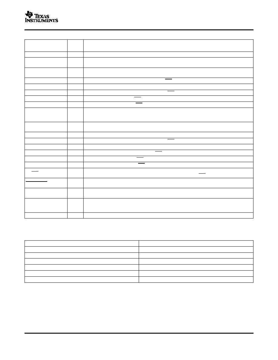
Terminal Functions
TERMINAL
I/O
DESCRIPTION
NAME
NO.
BYPASS
11
Tap to voltage divider for internal mid-supply bias generator
If a 47-nF capacitor is attached, the TPA0132 generates an internal clock. An external clock can
CLK
17
I
override the internal clock input to this terminal.
1, 12
GND
I
Ground connection for circuitry. Connected to thermal pad
13, 24
LHPIN
6
I
Left channel headphone input, selected when SE/BTL is held high
LIN
10
I
Common left input for fully differential input. AC ground for single-ended inputs.
LLINEIN
5
I
Left channel line negative input, selected when SE/BTL is held low
LOUT+
4
O
Left channel positive output in BTL mode and positive output in SE mode
LOUT-
9
O
Left channel negative output in BTL mode and high-impedance in SE mode
If this terminal is high, the detection circuitry for PC-BEEP is overridden and passes PC-BEEP through
PCB ENABLE
2
I
the amplifier, regardless of its amplitude. If PCB ENABLE is floating or low, the amplifier continues to
operate normally.
The input for PC-Beep mode. PC-BEEP is enabled when a > 1.5-V (peak-to-peak) square wave is
PC-BEEP
14
I
input to PC-BEEP or PCB ENABLE is high.
PVDD
7, 18
I
Power supply for output stage
RHPIN
20
I
Right channel headphone input, selected when SE/BTL is held high
RIN
8
I
Common right input for fully differential input. AC ground for single-ended inputs.
RLINEIN
23
I
Right channel line input, selected when SE/BTL is held low
ROUT+
21
O
Right channel positive output in BTL mode and positive output in SE mode
ROUT-
16
O
Right channel negative output in BTL mode and high-impedance in SE mode
Input and output MUX control. When this terminal is held high, the LHPIN or RHPIN and SE output is
SE/BTL
15
I
selected. When this terminal is held low, the LLINEIN or RLINEIN and BTL output are selected.
When held low, this terminal places the entire device, except PC-BEEP detect circuitry, in shutdown
SHUTDOWN
22
I
mode.
Analog VDD input supply. This terminal needs to be isolated from PVDD to achieve highest
VDD
19
I
performance.
VOLUME detects the dc level at the terminal and sets the gain for 31 discrete steps covering a range
VOLUME
3
I
of 20 dB to -40 dB for dc levels of 0.15 V to 3.54 V. When the dc level is over 3.54 V, the device is
muted.
Thermal Pad
Connect to ground. Must be soldered down in all applications to properly secure device on PC board.
over operating free-air temperature range (unless otherwise noted)
Supply voltage, VDD
6 V
Input voltage, VI
-0.3 V to VDD 0.3 V
Continuous total power dissipation
Internally limited (see Dissipation Rating Table)
Operating free-air temperature range, TA
-40
°C to 85°C
Operating junction temperature range, TJ
-40
°C to 150°C
Storage temperature range, Tstg
-65
°C to 85°C
Lead temperature 1,6 mm (1/16 inch) from case for 10 seconds
260
°C
(1)
Stresses beyond those listed under "absolute maximum ratings” may cause permanent damage to the device. These are stress ratings
only, and functional operation of the device at these or any other conditions beyond those indicated under "recommended operating
conditions” is not implied. Exposure to absolute-maximum-rated conditions for extended periods may affect device reliability.
3
相關PDF資料 |
PDF描述 |
|---|---|
| TPA0142PWPR | 2 CHANNEL(S), VOLUME CONTROL CIRCUIT, PDSO24 |
| TPA0142PWP | 2 CHANNEL(S), VOLUME CONTROL CIRCUIT, PDSO24 |
| TPA0142PWPG4 | 2 CHANNEL(S), VOLUME CONTROL CIRCUIT, PDSO24 |
| TPA0142PWPRG4 | 2 CHANNEL(S), VOLUME CONTROL CIRCUIT, PDSO24 |
| TPA0152PWPR | 2 CHANNEL(S), VOLUME CONTROL CIRCUIT, PDSO24 |
相關代理商/技術參數 |
參數描述 |
|---|---|
| TPA0142 | 制造商:TI 制造商全稱:Texas Instruments 功能描述:2-W STEREO AUDIO POWER AMPLIFIER WITH DC VOLUME CONTROL |
| TPA0142EVM | 功能描述:音頻 IC 開發工具 TPA0142 Eval Mod RoHS:否 制造商:Texas Instruments 產品:Evaluation Kits 類型:Audio Amplifiers 工具用于評估:TAS5614L 工作電源電壓:12 V to 38 V |
| TPA0142PWP | 功能描述:音頻放大器 2W Stereo A RoHS:否 制造商:STMicroelectronics 產品:General Purpose Audio Amplifiers 輸出類型:Digital 輸出功率: THD + 噪聲: 工作電源電壓:3.3 V 電源電流: 最大功率耗散: 最大工作溫度: 安裝風格:SMD/SMT 封裝 / 箱體:TQFP-64 封裝:Reel |
| TPA0142PWPG4 | 功能描述:音頻放大器 2W Stereo APA With DC Volume Control RoHS:否 制造商:STMicroelectronics 產品:General Purpose Audio Amplifiers 輸出類型:Digital 輸出功率: THD + 噪聲: 工作電源電壓:3.3 V 電源電流: 最大功率耗散: 最大工作溫度: 安裝風格:SMD/SMT 封裝 / 箱體:TQFP-64 封裝:Reel |
| TPA0142PWPR | 功能描述:音頻放大器 2W Stereo APA With DC Volume Control RoHS:否 制造商:STMicroelectronics 產品:General Purpose Audio Amplifiers 輸出類型:Digital 輸出功率: THD + 噪聲: 工作電源電壓:3.3 V 電源電流: 最大功率耗散: 最大工作溫度: 安裝風格:SMD/SMT 封裝 / 箱體:TQFP-64 封裝:Reel |
發布緊急采購,3分鐘左右您將得到回復。