- 您現(xiàn)在的位置:買賣IC網(wǎng) > PDF目錄382675 > TPS23841_07 (Texas Instruments, Inc.) HIGH-POWER, WIDE VOLTAGE RANGE, QUAD-PORT ETHERNET POWER SOURCING EQUIPMENT MANAGER PDF資料下載
參數(shù)資料
| 型號(hào): | TPS23841_07 |
| 廠商: | Texas Instruments, Inc. |
| 英文描述: | HIGH-POWER, WIDE VOLTAGE RANGE, QUAD-PORT ETHERNET POWER SOURCING EQUIPMENT MANAGER |
| 中文描述: | 大功率,寬電壓范圍,四端口以太網(wǎng)供電設(shè)備管理器 |
| 文件頁(yè)數(shù): | 9/52頁(yè) |
| 文件大小: | 1011K |
| 代理商: | TPS23841_07 |
第1頁(yè)第2頁(yè)第3頁(yè)第4頁(yè)第5頁(yè)第6頁(yè)第7頁(yè)第8頁(yè)當(dāng)前第9頁(yè)第10頁(yè)第11頁(yè)第12頁(yè)第13頁(yè)第14頁(yè)第15頁(yè)第16頁(yè)第17頁(yè)第18頁(yè)第19頁(yè)第20頁(yè)第21頁(yè)第22頁(yè)第23頁(yè)第24頁(yè)第25頁(yè)第26頁(yè)第27頁(yè)第28頁(yè)第29頁(yè)第30頁(yè)第31頁(yè)第32頁(yè)第33頁(yè)第34頁(yè)第35頁(yè)第36頁(yè)第37頁(yè)第38頁(yè)第39頁(yè)第40頁(yè)第41頁(yè)第42頁(yè)第43頁(yè)第44頁(yè)第45頁(yè)第46頁(yè)第47頁(yè)第48頁(yè)第49頁(yè)第50頁(yè)第51頁(yè)第52頁(yè)
www.ti.com
TPS23841
SLUS745–NOVEMBER 2006
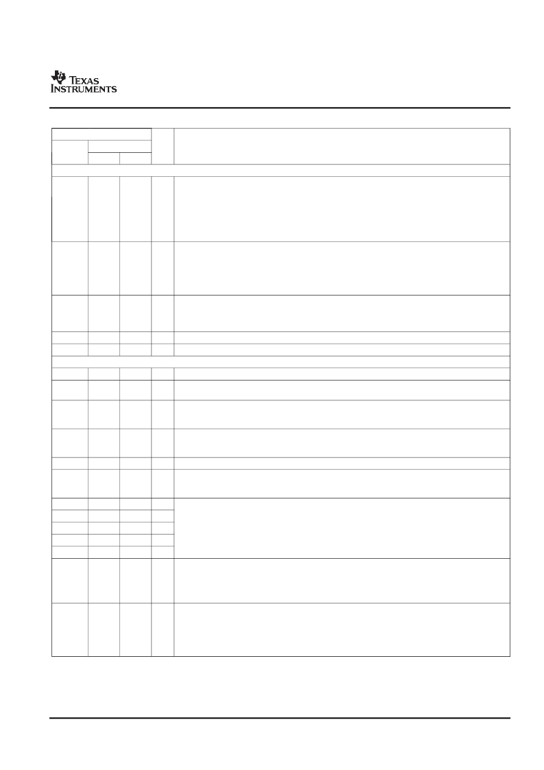
TERMINAL FUNCTIONS (continued)
TERMINAL
NO.
I/O
DESCRIPTION
NAME
PAP
PJD
ANALOG SIGNALS
This is a dual-purpose pin. When tied to an external capacitor this pin sets the internal clock. When
the CT pin is grounded the SYN pin turns from a output to an input (see SYN pin description)
The timing capacitor and the resistor on the RBIAS pin sets the internal clock frequency of the
device. This internal clock is used for the internal state machine, integrating A/D counters, POR time
out, faults and delay timers of each port. Using a 220-pF capacitor for CT and a 124-k
resistor for
RBIAS sets the internal clock to 245 kHz and ensure IEEE 802.3af compliance along with maximizing
the rejection of 60-Hz line frequency noise from A/D measurements.
Bias set resistor. This resistor sets all precision bias currents within the chip. This pin will regulate to
1.25V (V2.5/2) when a resistor is connected between RBIAS and RG. This voltage and RBIAS
generate a current which is replicated and used throughout the chip. This resistor also works in
conjunction with the capacitors on CT and CINT to set internal timing values. The RBIAS resistor
should be connected RG. RBIAS is a high impedance input and care needs to be taken to avoid
signal injection from the SYN pin or I
2
C signals.
This is a dual purpose pin. When the CT pin is connected to a timing capacitor this output pin is a 0v
to 3.3V pulse of the internal clock which can be used to drive other TPS23841 SYN pins for
elimination of a timing capacitor. When the CT pin is grounded this pin becomes an input pin that can
be driven from a master TPS23841 or any other clock generator signal.
Totem-pole output pin for AC Disconnect excitation.
Totem-pole output pin for AC Disconnect excitation.
CT
53
12
I
RBIAS
55
10
I
SYN
52
13
I/O
AC_LO
AC_HI
DIGITAL SIGNALS
SCL
51
50
14
15
O
O
25
40
I
Serial clock input pin for the I
2
C interface.
Serial data input pin for the I
2
C interface. When tied to the SDA_O pin, this connection becomes the
standard bi-directional serial data line (SDA)
Serial data open drain output for the I
2
C interface. When tied to the SDA_I pin, this connection
becomes the standard bi-directional serial data line (SDA). This is a open drain output that can
directly drive opto-coupler.
The WD_DIS pin disables the watchdog timer function when connected to 3.3 V. The pin has internal
50-k. resistor to digital ground. The watchdog timer monitors the I
2
C clock pin (SCL) and the internal
oscillator activity in power management mode and only the internal oscillator activity in auto mode.
This is an open-drain output that goes low if a fault condition occurs on any of the 4 ports.
When this input is set to logic low there is no back-off time after a discovery failure. When this pin set
to a logic high there is a back-off time (approximately 2 seconds) before initiating another discovery
cycle. This pin has an internal 50-k
resistor pull-down to digital ground.
SDA_I
26
39
I
SDA_O
27
38
O
WD_DIS
22
43
I
INTB
20
45
O
ALTA/B
21
44
I
A1
A2
A3
A4
A5
28
29
30
31
32
37
36
35
34
33
I
I
I
I
I
Address 1 through 5 These are the I
2
C address select inputs. Select the appropriate binary address
on these pins by connecting to the chip ground for a logic low or tying to the V3.3 pin for a logic high.
Each address line has an internal current source pull-down to digital ground.
The MS pin selects either the auto mode (MS low) or the power management mode, PMM, (MS
high). This pin can be held low for controller-less standalone applications. When MS is low and the
POR timing cycle is complete the chip will sequentially
Discover, Classify and Power on
each port.
When MS is set high the ports are controlled by register setting via the I
2
C bus. The MS pin has an
internal 50-k
resistor pull-down to analog ground.
This pin can be used to override the internal POR. When held low, the I
2
C interface, all the state
machines, and registers are held in reset. When all internal and external supplies are within
specification, and this pin is set to a logic high level, the POR delay will begin. The I
2
C interface and
registers will become active within 70
μ
s of this event and communications to read or preset registers
can begin. The reset delay for the remainder of the chip then extinguishes in 1 second. This pin has
an internal 50-k
resistor pull-down to analog ground.
MS
63
2
I
PORB
62
3
I
9
Submit Documentation Feedback
相關(guān)PDF資料 |
PDF描述 |
|---|---|
| TPS252 | PHOTOVOLTAIC CELL FOR THERMOPILE DETECTION |
| TPS2524 | PHOTOVOLTAIC CELL FOR THERMOPILE DETECTION |
| TPS252G1 | PHOTOVOLTAIC CELL FOR THERMOPILE DETECTION |
| TPS252G10 | PHOTOVOLTAIC CELL FOR THERMOPILE DETECTION |
| TPS252G12 | PHOTOVOLTAIC CELL FOR THERMOPILE DETECTION |
相關(guān)代理商/技術(shù)參數(shù) |
參數(shù)描述 |
|---|---|
| TPS23841PAP | 功能描述:熱插拔功率分布 HP Wide Volt Range Quad Part Ethernet RoHS:否 制造商:Texas Instruments 產(chǎn)品:Controllers & Switches 電流限制: 電源電壓-最大:7 V 電源電壓-最小:- 0.3 V 工作溫度范圍: 功率耗散: 安裝風(fēng)格:SMD/SMT 封裝 / 箱體:MSOP-8 封裝:Tube |
| TPS23841PAPG4 | 功能描述:熱插拔功率分布 HP Wide Volt Range Quad Part Ethernet RoHS:否 制造商:Texas Instruments 產(chǎn)品:Controllers & Switches 電流限制: 電源電壓-最大:7 V 電源電壓-最小:- 0.3 V 工作溫度范圍: 功率耗散: 安裝風(fēng)格:SMD/SMT 封裝 / 箱體:MSOP-8 封裝:Tube |
| TPS23841PAPR | 功能描述:熱插拔功率分布 HP Wide Volt Range Quad Part Ethernet RoHS:否 制造商:Texas Instruments 產(chǎn)品:Controllers & Switches 電流限制: 電源電壓-最大:7 V 電源電壓-最小:- 0.3 V 工作溫度范圍: 功率耗散: 安裝風(fēng)格:SMD/SMT 封裝 / 箱體:MSOP-8 封裝:Tube |
| TPS23841PAPRG4 | 功能描述:熱插拔功率分布 HP Wide Volt Range Quad Part Ethernet RoHS:否 制造商:Texas Instruments 產(chǎn)品:Controllers & Switches 電流限制: 電源電壓-最大:7 V 電源電壓-最小:- 0.3 V 工作溫度范圍: 功率耗散: 安裝風(fēng)格:SMD/SMT 封裝 / 箱體:MSOP-8 封裝:Tube |
| TPS23841PJD | 功能描述:熱插拔功率分布 HP Wide Volt Range Quad Part Ethernet RoHS:否 制造商:Texas Instruments 產(chǎn)品:Controllers & Switches 電流限制: 電源電壓-最大:7 V 電源電壓-最小:- 0.3 V 工作溫度范圍: 功率耗散: 安裝風(fēng)格:SMD/SMT 封裝 / 箱體:MSOP-8 封裝:Tube |
發(fā)布緊急采購(gòu),3分鐘左右您將得到回復(fù)。