- 您現在的位置:買賣IC網 > PDF目錄98282 > TPS54110PWPG4 (TEXAS INSTRUMENTS INC) 3.5 A SWITCHING REGULATOR, 762 kHz SWITCHING FREQ-MAX, PDSO20 PDF資料下載
參數資料
| 型號: | TPS54110PWPG4 |
| 廠商: | TEXAS INSTRUMENTS INC |
| 元件分類: | 穩壓器 |
| 英文描述: | 3.5 A SWITCHING REGULATOR, 762 kHz SWITCHING FREQ-MAX, PDSO20 |
| 封裝: | GREEN, PLASTIC, HTSSOP-20 |
| 文件頁數: | 30/30頁 |
| 文件大小: | 870K |
| 代理商: | TPS54110PWPG4 |
第1頁第2頁第3頁第4頁第5頁第6頁第7頁第8頁第9頁第10頁第11頁第12頁第13頁第14頁第15頁第16頁第17頁第18頁第19頁第20頁第21頁第22頁第23頁第24頁第25頁第26頁第27頁第28頁第29頁當前第30頁
(
)
D
+
0.25
OUT(MAX)
=
IN
MAX
OUT(MAX)
BULK
SW
I
V
I
ESR
C
OUT(MAX)
CIN
I
2
=
(
)
F
)
IN(MAX
OUT
MIN
IND
OUT
IN(MAX)
SW
V
-V
L
V
K
I
=
SLVS500C
– DECEMBER 2003 – REVISED FEBRUARY 2011
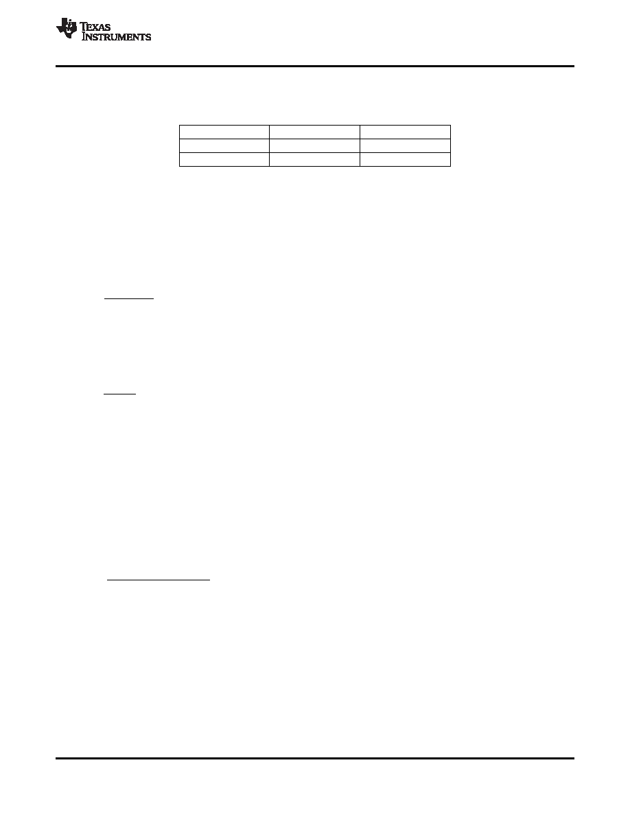
Alternately, the TPS54110 can be set to preprogrammed switching frequencies of 350 kHz or 550 kHz by
connecting pins RT and SYNC as shown in Table 2.
Table 2. Design Parameters
FREQUENCY
RT
SYNC
350 kHz
Float
Float or AGND
550 kHz
Float
≥ 2.5 V
Input Capacitors
The TPS54110 requires an input decoupling capacitor and, depending on the application, a bulk input capacitor.
The minimum value for the decoupling capacitor, C9, is 10 uF. A high quality ceramic type X5R or X7R with a
voltage rating greater than the maximum input voltage is recommended. A bulk input capacitor may be needed,
especially if the TPS54110 circuit is not located within approximately 2 inches from the input voltage source. The
capacitance value is not critical, but the voltage rating must be greater than the maximum input voltage including
ripple voltage. The capacitor must filter the input ripple voltage to acceptable levels.
Input ripple voltage can be approximated by Equation 2:
(2)
Where
IOUT(MAX) is the maximum load current,
SW is the switching frequency, CBULK is the bulk capacitor value and
ESRMAX is the maximum series resistance of the bulk capacitor.
Worst-case RMS ripple current is approximated by Equation 3:
(3)
In this case the input ripple voltage is 66 mV with a 10-
F bulk capacitor. Figure 15 shows the measured ripple
waveform. The RMS ripple current is 0.75 A. The maximum voltage across the input capacitors is VINMAX +
ΔVIN/2. The bypass capacitor and input bulk capacitor are each rated for 6.3 V and a ripple-current capacity of
1.5 A, providing some margin. It is very important that the maximum ratings for voltage and current are not
exceeded under any circumstance.
Output Filter Components
Two
components,
L1
and
C2,
are
selected
for
the
output
filter.
Since
the
TPS54110
is
an
externally-compensated device, a wide range of filter-component types and values are supported.
Inductor Selection
Use Equation 4 to calculate the minimum value of the output inductor:
(4)
KIND is a coefficient that represents the amount of inductor ripple current relative to the maximum output current.
For designs using low-ESR capacitors such as ceramics, use KIND = 0.2. When using higher ESR output
capacitors, KIND = 0.1 yields better results. If higher ripple currents can be tolerated, KIND can be increased
allowing for a smaller output-inductor value.
This example design uses KIND = 0.2, yielding a minimum inductor value of 6.29 H. The next-higher standard
value of 6.8
H is chosen for this design. If a lower inductor value is desired, a larger amount of ripple current
must be tolerated.
The RMS-current and saturation-current ratings of the output filter inductor must not be exceeded. The RMS
inductor current can be found from Equation 5:
2003–2011, Texas Instruments Incorporated
9
Product Folder Link(s): TPS54110
相關PDF資料 |
PDF描述 |
|---|---|
| TPS54140QDRCRQ1 | SWITCHING REGULATOR, PDSO10 |
| TPS54160DRCT | SWITCHING REGULATOR, 2500 kHz SWITCHING FREQ-MAX, PDSO10 |
| TPS54160DGQ | 2.7 A SWITCHING REGULATOR, 2500 kHz SWITCHING FREQ-MAX, PDSO10 |
| TPS54160DGQR | 2.7 A SWITCHING REGULATOR, 2500 kHz SWITCHING FREQ-MAX, PDSO10 |
| TPS5420MDREPG4 | 5.2 A SWITCHING REGULATOR, 600 kHz SWITCHING FREQ-MAX, PDSO8 |
相關代理商/技術參數 |
參數描述 |
|---|---|
| TPS54110PWPR | 功能描述:直流/直流開關調節器 1.5A Step Down Converter RoHS:否 制造商:International Rectifier 最大輸入電壓:21 V 開關頻率:1.5 MHz 輸出電壓:0.5 V to 0.86 V 輸出電流:4 A 輸出端數量: 最大工作溫度: 安裝風格:SMD/SMT 封裝 / 箱體:PQFN 4 x 5 |
| TPS54110PWPRG4 | 功能描述:直流/直流開關調節器 1.5A Step Down Converter RoHS:否 制造商:International Rectifier 最大輸入電壓:21 V 開關頻率:1.5 MHz 輸出電壓:0.5 V to 0.86 V 輸出電流:4 A 輸出端數量: 最大工作溫度: 安裝風格:SMD/SMT 封裝 / 箱體:PQFN 4 x 5 |
| TPS54110-Q1 | 制造商:TI 制造商全稱:Texas Instruments 功能描述:3-V TO 6-V INPUT, 1.5-A OUTPUT SYNCHRONOUS-BUCK PWM SWITCHER WITH INTEGRATED FETs (SWIFT?£a) |
| TPS54110QPWPRQ1 | 功能描述:直流/直流開關調節器 3-6V Input 1.5A Out Synch Buck PWM Swer RoHS:否 制造商:International Rectifier 最大輸入電壓:21 V 開關頻率:1.5 MHz 輸出電壓:0.5 V to 0.86 V 輸出電流:4 A 輸出端數量: 最大工作溫度: 安裝風格:SMD/SMT 封裝 / 箱體:PQFN 4 x 5 |
| TPS54112PWP | 制造商:Texas Instruments 功能描述: |
發布緊急采購,3分鐘左右您將得到回復。