- 您現在的位置:買賣IC網 > PDF目錄98282 > TPS54160DRCT (TEXAS INSTRUMENTS INC) SWITCHING REGULATOR, 2500 kHz SWITCHING FREQ-MAX, PDSO10 PDF資料下載
參數資料
| 型號: | TPS54160DRCT |
| 廠商: | TEXAS INSTRUMENTS INC |
| 元件分類: | 穩(wěn)壓器 |
| 英文描述: | SWITCHING REGULATOR, 2500 kHz SWITCHING FREQ-MAX, PDSO10 |
| 封裝: | PLASTIC, SON-10 |
| 文件頁數: | 33/50頁 |
| 文件大小: | 1375K |
| 代理商: | TPS54160DRCT |
第1頁第2頁第3頁第4頁第5頁第6頁第7頁第8頁第9頁第10頁第11頁第12頁第13頁第14頁第15頁第16頁第17頁第18頁第19頁第20頁第21頁第22頁第23頁第24頁第25頁第26頁第27頁第28頁第29頁第30頁第31頁第32頁當前第33頁第34頁第35頁第36頁第37頁第38頁第39頁第40頁第41頁第42頁第43頁第44頁第45頁第46頁第47頁第48頁第49頁第50頁
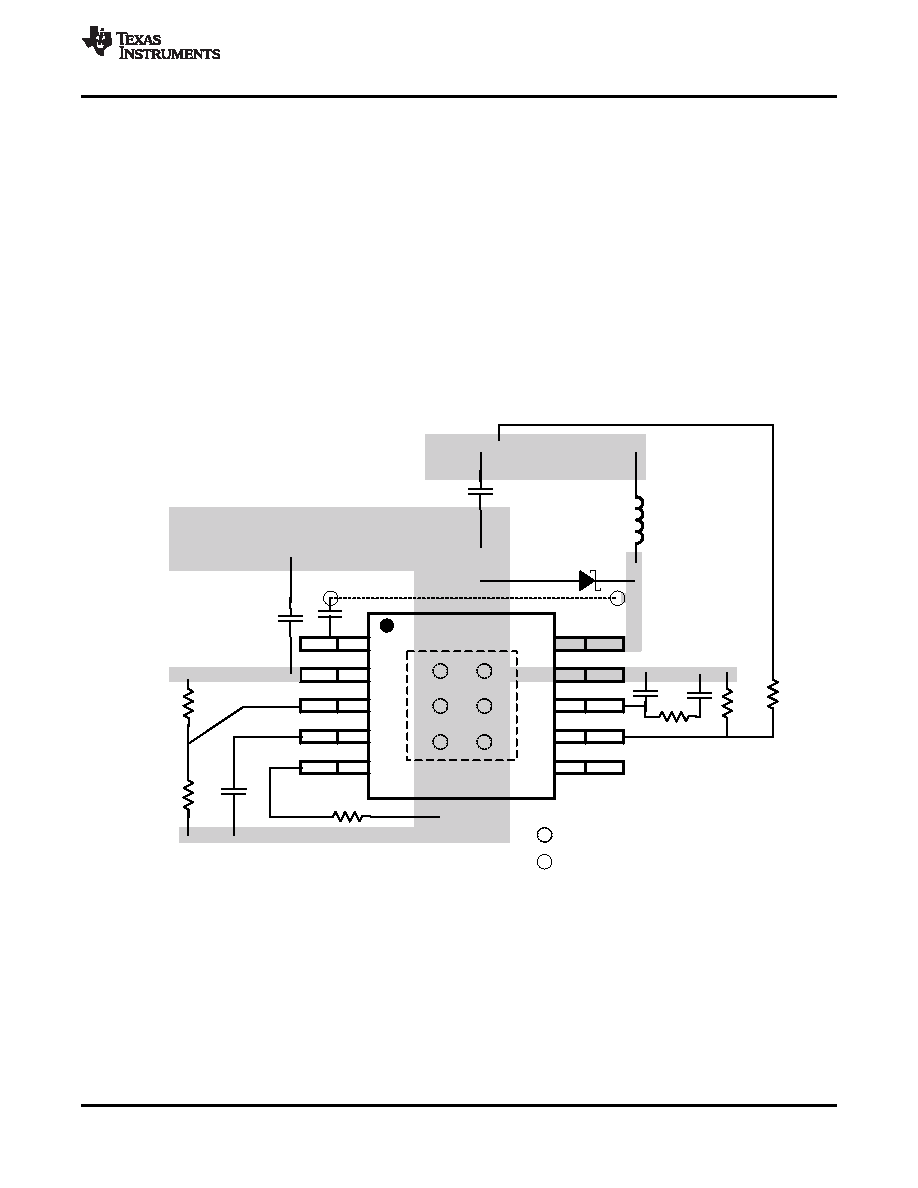
BOOT
VIN
EN
SS/TR
RT/CLK
PH
GND
COMP
VSENSE
PWRGD
Input
Bypass
Capacitor
UVLO
Adjust
Resistors
SlowStart
Capacitor
Frequency
SetResistor
Compensation
Network
Resistor
Divider
Output
Inductor
Output
Capacitor
Vout
Vin
Topside
Ground
Area
Catch
Diode
RouteBootCapacitor
Traceonanotherlayerto
providewidepathfor
topsideground
ThermalVIA
SignalVIA
www.ti.com
SLVS795C – OCTOBER 2008 – REVISED OCTOBER 2010
Layout
Layout is a critical portion of good power supply design. There are several signals paths that conduct fast
changing currents or voltages that can interact with stray inductance or parasitic capacitance to generate noise
or degrade the power supplies performance. To help eliminate these problems, the VIN pin should be bypassed
to ground with a low ESR ceramic bypass capacitor with X5R or X7R dielectric. Care should be taken to
minimize the loop area formed by the bypass capacitor connections, the VIN pin, and the anode of the catch
diode. See Figure 65 for a PCB layout example. The GND pin should be tied directly to the power pad under the
device and the power pad.
The power pad should be connected to any internal PCB ground planes using multiple vias directly under the
device. The PH pin should be routed to the cathode of the catch diode and to the output inductor. Since the PH
connection is the switching node, the catch diode and output inductor should be located close to the PH pins,
and the area of the PCB conductor minimized to prevent excessive capacitive coupling. For operation at full rated
load, the top side ground area must provide adequate heat dissipating area. The RT/CLK pin is sensitive to noise
so the RT resistor should be located as close as possible to the device and routed with minimal lengths of trace.
The additional external components can be placed approximately as shown. It may be possible to obtain
acceptable performance with alternate PCB layouts, however this layout has been shown to produce good
results and is meant as a guideline.
Figure 65. PCB Layout Example
Copyright 2008–2010, Texas Instruments Incorporated
39
Product Folder Link(s): TPS54160
相關PDF資料 |
PDF描述 |
|---|---|
| TPS54160DGQ | 2.7 A SWITCHING REGULATOR, 2500 kHz SWITCHING FREQ-MAX, PDSO10 |
| TPS54160DGQR | 2.7 A SWITCHING REGULATOR, 2500 kHz SWITCHING FREQ-MAX, PDSO10 |
| TPS5420MDREPG4 | 5.2 A SWITCHING REGULATOR, 600 kHz SWITCHING FREQ-MAX, PDSO8 |
| TPS5420MDREP | 5.2 A SWITCHING REGULATOR, 600 kHz SWITCHING FREQ-MAX, PDSO8 |
| TPS54225PWP | 4.5 A SWITCHING REGULATOR, 700 kHz SWITCHING FREQ-MAX, PDSO14 |
相關代理商/技術參數 |
參數描述 |
|---|---|
| TPS54160EVM-230 | 功能描述:電源管理IC開發(fā)工具 TPS54160 Eval Mod RoHS:否 制造商:Maxim Integrated 產品:Evaluation Kits 類型:Battery Management 工具用于評估:MAX17710GB 輸入電壓: 輸出電壓:1.8 V |
| TPS54160EVM-535 | 功能描述:電源管理IC開發(fā)工具 Eval Mod for High Brightness LED Drvr RoHS:否 制造商:Maxim Integrated 產品:Evaluation Kits 類型:Battery Management 工具用于評估:MAX17710GB 輸入電壓: 輸出電壓:1.8 V |
| TPS54160-Q1 | 制造商:TI 制造商全稱:Texas Instruments 功能描述:1.5-A 60-V STEP-DOWN SWIFT DC/DC CONVERTER WITH Eco-Mode CONTROL |
| TPS54160QDGQRDL | 制造商:Texas Instruments 功能描述:- Tape and Reel |
| TPS54160QDGQRQ1 | 功能描述:直流/直流開關調節(jié)器 Aut Cat 3.5-60V 1.5A Step Down Converter RoHS:否 制造商:International Rectifier 最大輸入電壓:21 V 開關頻率:1.5 MHz 輸出電壓:0.5 V to 0.86 V 輸出電流:4 A 輸出端數量: 最大工作溫度: 安裝風格:SMD/SMT 封裝 / 箱體:PQFN 4 x 5 |
發(fā)布緊急采購,3分鐘左右您將得到回復。