- 您現在的位置:買賣IC網 > PDF目錄98283 > TPS54331DG4 (TEXAS INSTRUMENTS INC) 2 A SWITCHING REGULATOR, 684 kHz SWITCHING FREQ-MAX, PDSO8 PDF資料下載
參數資料
| 型號: | TPS54331DG4 |
| 廠商: | TEXAS INSTRUMENTS INC |
| 元件分類: | 穩壓器 |
| 英文描述: | 2 A SWITCHING REGULATOR, 684 kHz SWITCHING FREQ-MAX, PDSO8 |
| 封裝: | GREEN, PLASTIC, MS-012AA, SOIC-8 |
| 文件頁數: | 26/27頁 |
| 文件大小: | 794K |
| 代理商: | TPS54331DG4 |
第1頁第2頁第3頁第4頁第5頁第6頁第7頁第8頁第9頁第10頁第11頁第12頁第13頁第14頁第15頁第16頁第17頁第18頁第19頁第20頁第21頁第22頁第23頁第24頁第25頁當前第26頁第27頁
EN
1.25V
VIN
+
-
Ren1
Ren2
TPS54331
1
A
m
3
A
m
START
STOP
V
- V
Ren1 =
3
A
m
EN
START
EN
V
Ren2 =
V
- V
+ 1
A
Ren1
m
(
)
( )
(
)
SS
ref
SS
C
nF
V
T
ms
=
I
A
m
SLVS839C – JULY 2008 – REVISED MARCH 2010
www.ti.com
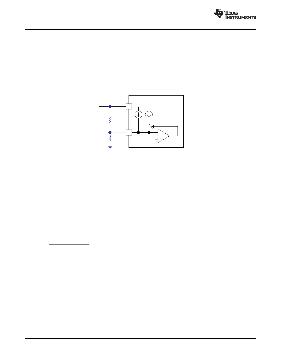
ENABLE AND ADJUSTABLE INPUT UNDER-VOLTAGE LOCKOUT (VIN UVLO)
The EN pin has an internal pull-up current source that provides the default condition of the TPS54331 operating
when the EN pin floats.
The TPS54331 is disabled when the VIN pin voltage falls below internal VIN UVLO threshold. It is recommended
to use an external VIN UVLO to add Hysteresis unless VIN is greater than (VOUT + 2 V). To adjust the VIN UVLO
with Hysteresis, use the external circuitry connected to the EN pin as shown in Figure 12. Once the EN pin
voltage exceeds 1.25 V, an additional 3 mA of hysteresis is added. Use Equation 1 and Equation 2 to calculate
the resistor values needed for the desired VIN UVLO threshold voltages. The VSTART is the input start threshold
voltage, the VSTOP is the input stop threshold voltage and the VEN is the enable threshold voltage of 1.25 V. The
VSTOP should always be greater than 3.5 V.
Figure 12. Adjustable Input Undervoltage Lockout
(1)
(2)
PROGRAMMABLE SLOW START USING SS PIN
It is highly recommended to program the slow start time externally because no slow start time is implemented
internally. The TPS54331 effectively uses the lower voltage of the internal voltage reference or the SS pin
voltage as the power supply’s reference voltage fed into the error amplifier and will regulate the output
accordingly. A capacitor (CSS) on the SS pin to ground implements a slow start time. The TPS54331 has an
internal pull-up current source of 2mA that charges the external slow start capacitor. The equation for the slow
(3)
The slow start time should be set between 1ms to 10 ms to ensure good start-up behavior. The slow start
capacitor should be no more than 27nF.
If during normal operation, the input voltage drops below the VIN UVLO threshold, or the EN pin is pulled below
1.25 V, or a thermal shutdown event occurs, the TPS54331 stops switching.
ERROR AMPLIFIER
The TPS54331 has a transconductance amplifier for the error amplifier. The error amplifier compares the
VSENSE voltage to the internal effective voltage reference presented at the input of the error amplifier. The
transconductance of the error amplifier is 92 mA/V during normal operation. Frequency compensation
components are connected between the COMP pin and ground.
SLOPE COMPENSATION
In order to prevent the sub-harmonic oscillations when operating the device at duty cycles greater than 50%, the
TPS54331 adds a built-in slope compensation which is a compensating ramp to the switch current signal.
8
Copyright 2008–2010, Texas Instruments Incorporated
Product Folder Link(s): TPS54331
相關PDF資料 |
PDF描述 |
|---|---|
| TPS54350MPWPREP | 7.2 A SWITCHING REGULATOR, 700 kHz SWITCHING FREQ-MAX, PDSO16 |
| TPS54372PWP | 3 A SWITCHING REGULATOR, 762 kHz SWITCHING FREQ-MAX, PDSO20 |
| TPS54418RTER | 6.4 A SWITCHING REGULATOR, 2000 kHz SWITCHING FREQ-MAX, PQCC16 |
| TPS54426PWP | 7.5 A SWITCHING REGULATOR, 700 kHz SWITCHING FREQ-MAX, PDSO14 |
| TPS54429PWP | 0.01 A SWITCHING REGULATOR, 700 kHz SWITCHING FREQ-MAX, PDSO14 |
相關代理商/技術參數 |
參數描述 |
|---|---|
| TPS54331DR | 功能描述:直流/直流開關轉換器 3A 28V In Step Down SWIFT DC/DC Cnvrtr RoHS:否 制造商:STMicroelectronics 最大輸入電壓:4.5 V 開關頻率:1.5 MHz 輸出電壓:4.6 V 輸出電流:250 mA 輸出端數量:2 最大工作溫度:+ 85 C 安裝風格:SMD/SMT |
| TPS54331DRG4 | 功能描述:直流/直流開關轉換器 26V,3A DC-DC Converter RoHS:否 制造商:STMicroelectronics 最大輸入電壓:4.5 V 開關頻率:1.5 MHz 輸出電壓:4.6 V 輸出電流:250 mA 輸出端數量:2 最大工作溫度:+ 85 C 安裝風格:SMD/SMT |
| TPS54331DR-P | 制造商:Rochester Electronics LLC 功能描述: 制造商:Texas Instruments 功能描述: |
| TPS54331EVM-232 | 功能描述:電源管理IC開發工具 SWIFT Cnvrtr Eval Mod RoHS:否 制造商:Maxim Integrated 產品:Evaluation Kits 類型:Battery Management 工具用于評估:MAX17710GB 輸入電壓: 輸出電壓:1.8 V |
| TPS54331EVM-232 | 制造商:Texas Instruments 功能描述:DEVELOPMENT TOOL |
發布緊急采購,3分鐘左右您將得到回復。