- 您現在的位置:買賣IC網 > PDF目錄98283 > TPS54331DG4 (TEXAS INSTRUMENTS INC) 2 A SWITCHING REGULATOR, 684 kHz SWITCHING FREQ-MAX, PDSO8 PDF資料下載
參數資料
| 型號: | TPS54331DG4 |
| 廠商: | TEXAS INSTRUMENTS INC |
| 元件分類: | 穩壓器 |
| 英文描述: | 2 A SWITCHING REGULATOR, 684 kHz SWITCHING FREQ-MAX, PDSO8 |
| 封裝: | GREEN, PLASTIC, MS-012AA, SOIC-8 |
| 文件頁數: | 27/27頁 |
| 文件大小: | 794K |
| 代理商: | TPS54331DG4 |
第1頁第2頁第3頁第4頁第5頁第6頁第7頁第8頁第9頁第10頁第11頁第12頁第13頁第14頁第15頁第16頁第17頁第18頁第19頁第20頁第21頁第22頁第23頁第24頁第25頁第26頁當前第27頁
www.ti.com
SLVS839C – JULY 2008 – REVISED MARCH 2010
CURRENT MODE COMPENSATION DESIGN
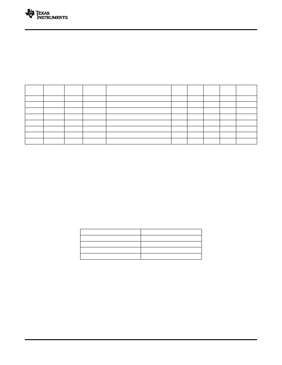
To simplify design efforts using the TPS54331, the typical designs for common applications are listed in Table 1.
For designs using ceramic output capacitors, proper derating of ceramic output capacitance is recommended
when doing the stability analysis. This is because the actual ceramic capacitance drops considerably from the
nominal value when the applied voltage increases. Advanced users may refer to the Step by Step Design
Procedure in the Application Information section for the detailed guidelines or use SwitcherPro Software tool
Table 1. Typical Designs (Referring to Simplified Schematic on page 1)
VIN
VOUT
Fsw
Lo
Co
RO1
RO2
C2
C1
R3
(V)
(kHz)
(mH)
(k
)
(k
)
(pF)
(k
)
12
5
570
6.8
Ceramic 33 mFx2
10
1.91
39
4700
49.9
12
3.3
570
6.8
Ceramic 47mFx2
10
3.24
47
1000
29.4
12
1.8
570
4.7
Ceramic 100 mF
10
8.06
68
5600
29.4
12
0.9
570
3.3
Ceramic 100 mFx2
10
80.6
56
5600
29.4
12
5
570
6.8
Aluminum 330 mF/160 m
10
1.91
68
120
29.4
12
3.3
570
6.8
Aluminum 470 mF/160 m
10
3.24
82
220
10
12
1.8
570
4.7
SP 100 mF/15 m
10
8.06
68
5600
29.4
12
0.9
570
3.3
SP 330 mF/12 m
10
80.6
100
1200
49.9
OVERCURRENT PROTECTION AND FREQUENCY SHIFT
The TPS54331 implements current mode control that uses the COMP pin voltage to turn off the high-side
MOSFET on a cycle by cycle basis. Every cycle the switch current and the COMP pin voltage are compared;
when the peak inductor current intersects the COMP pin voltage, the high-side switch is turned off. During
overcurrent conditions that pull the output voltage low, the error amplifier responds by driving the COMP pin high,
causing the switch current to increase. The COMP pin has a maximum clamp internally, which limit the output
current.
The TPS54331 provides robust protection during short circuits. There is potential for overcurrent runaway in the
output inductor during a short circuit at the output. The TPS54331 solves this issue by increasing the off time
during short circuit conditions by lowering the switching frequency. The switching frequency is divided by 8, 4, 2,
and 1 as the voltage ramps from 0 V to 0.8 V on VSENSE pin. The relationship between the switching frequency
and the VSENSE pin voltage is shown in Table 2.
Table 2. Switching Frequency Conditions
SWITCHING FREQUENCY
VSENSE PIN VOLTAGE
570 kHz
VSENSE
≥ 0.6 V
570 kHz / 2
0.6 V > VSENSE
≥ 0.4 V
570 kHz / 4
0.4 V > VSENSE
≥ 0.2 V
570 kHz / 8
0.2 V > VSENSE
OVERVOLTAGE TRANSIENT PROTECTION
The TPS54331 incorporates an overvoltage transient protection (OVTP) circuit to minimize output voltage
overshoot when recovering from output fault conditions or strong unload transients. The OVTP circuit includes an
overvoltage comparator to compare the VSENSE pin voltage and internal thresholds. When the VSENSE pin
voltage goes above 109% × Vref, the high-side MOSFET will be forced off. When the VSENSE pin voltage falls
below 107% × Vref, the high-side MOSFET will be enabled again.
THERMAL SHUTDOWN
The device implements an internal thermal shutdown to protect itself if the junction temperature exceeds 165°C.
The thermal shutdown forces the device to stop switching when the junction temperature exceeds the thermal
trip threshold. Once the die temperature decreases below 165°C, the device reinitiates the power up sequence.
Copyright 2008–2010, Texas Instruments Incorporated
9
Product Folder Link(s): TPS54331
相關PDF資料 |
PDF描述 |
|---|---|
| TPS54350MPWPREP | 7.2 A SWITCHING REGULATOR, 700 kHz SWITCHING FREQ-MAX, PDSO16 |
| TPS54372PWP | 3 A SWITCHING REGULATOR, 762 kHz SWITCHING FREQ-MAX, PDSO20 |
| TPS54418RTER | 6.4 A SWITCHING REGULATOR, 2000 kHz SWITCHING FREQ-MAX, PQCC16 |
| TPS54426PWP | 7.5 A SWITCHING REGULATOR, 700 kHz SWITCHING FREQ-MAX, PDSO14 |
| TPS54429PWP | 0.01 A SWITCHING REGULATOR, 700 kHz SWITCHING FREQ-MAX, PDSO14 |
相關代理商/技術參數 |
參數描述 |
|---|---|
| TPS54331DR | 功能描述:直流/直流開關轉換器 3A 28V In Step Down SWIFT DC/DC Cnvrtr RoHS:否 制造商:STMicroelectronics 最大輸入電壓:4.5 V 開關頻率:1.5 MHz 輸出電壓:4.6 V 輸出電流:250 mA 輸出端數量:2 最大工作溫度:+ 85 C 安裝風格:SMD/SMT |
| TPS54331DRG4 | 功能描述:直流/直流開關轉換器 26V,3A DC-DC Converter RoHS:否 制造商:STMicroelectronics 最大輸入電壓:4.5 V 開關頻率:1.5 MHz 輸出電壓:4.6 V 輸出電流:250 mA 輸出端數量:2 最大工作溫度:+ 85 C 安裝風格:SMD/SMT |
| TPS54331DR-P | 制造商:Rochester Electronics LLC 功能描述: 制造商:Texas Instruments 功能描述: |
| TPS54331EVM-232 | 功能描述:電源管理IC開發工具 SWIFT Cnvrtr Eval Mod RoHS:否 制造商:Maxim Integrated 產品:Evaluation Kits 類型:Battery Management 工具用于評估:MAX17710GB 輸入電壓: 輸出電壓:1.8 V |
| TPS54331EVM-232 | 制造商:Texas Instruments 功能描述:DEVELOPMENT TOOL |
發布緊急采購,3分鐘左右您將得到回復。