- 您現在的位置:買賣IC網 > PDF目錄98283 > TPS54418RTER (TEXAS INSTRUMENTS INC) 6.4 A SWITCHING REGULATOR, 2000 kHz SWITCHING FREQ-MAX, PQCC16 PDF資料下載
參數資料
| 型號: | TPS54418RTER |
| 廠商: | TEXAS INSTRUMENTS INC |
| 元件分類: | 穩壓器 |
| 英文描述: | 6.4 A SWITCHING REGULATOR, 2000 kHz SWITCHING FREQ-MAX, PQCC16 |
| 封裝: | 3 X 3 MM, GREEN, PLASTIC, WQFN-16 |
| 文件頁數: | 2/35頁 |
| 文件大小: | 1356K |
| 代理商: | TPS54418RTER |
第1頁當前第2頁第3頁第4頁第5頁第6頁第7頁第8頁第9頁第10頁第11頁第12頁第13頁第14頁第15頁第16頁第17頁第18頁第19頁第20頁第21頁第22頁第23頁第24頁第25頁第26頁第27頁第28頁第29頁第30頁第31頁第32頁第33頁第34頁第35頁
RDSON-StaticDrain-SourecOnStateResistance-
W
0
20
40
60
80
100
120
140
160
180
200
-50
-25
0
25
50
75
100
125
150
T -JunctionTemperature-°C
J
V
=3.3V
IN
SLVS946A – MAY 2009 – REVISED MAY 2010
www.ti.com
TYPICAL CHARACTERISTICS CURVES (continued)
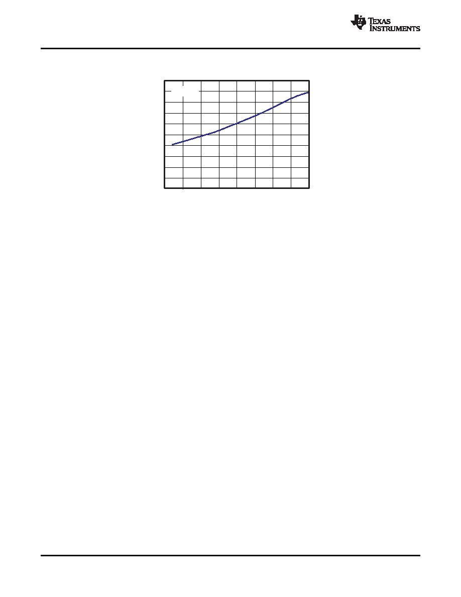
PWRGD ON RESISTANCE vs TEMPERATURE
Figure 21.
OVERVIEW
The TPS54418 is a 6-V, 4-A, synchronous step-down (buck) converter with two integrated n-channel MOSFETs.
To improve performance during line and load transients the device implements a constant frequency, peak
current mode control which reduces output capacitance and simplifies external frequency compensation design.
The wide switching frequency of 200 kHz to 2000 kHz allows for efficiency and size optimization when selecting
the output filter components. The switching frequency is adjusted using a resistor to ground on the RT/CLK pin.
The device has an internal phase lock loop (PLL) on the RT/CLK pin that is used to synchronize the power
switch turn on to a falling edge of an external system clock.
The TPS54418 has a typical default start up voltage of 2.6 V. The EN pin has an internal pull-up current source
that can be used to adjust the input voltage under voltage lockout (UVLO) with two external resistors. In addition,
the pull up current provides a default condition when the EN pin is floating for the device to operate. The total
operating current for the TPS54418 is 350 mA when not switching and under no load. When the device is
disabled, the supply current is less than 5 mA.
The integrated 30 m
MOSFETs allow for high efficiency power supply designs with continuous output currents
up to 4 amperes.
The TPS54418 reduces the external component count by integrating the boot recharge diode. The bias voltage
for the integrated high side MOSFET is supplied by a capacitor on the BOOT to PH pin. The boot capacitor
voltage is monitored by an UVLO circuit and turns off the high side MOSFET when the voltage falls below a
preset threshold. This BOOT circuit allows the TPS54418 to operate approaching 100%. The output voltage can
be stepped down to as low as the 0.8 V reference.
The TPS54418 has a power good comparator (PWRGD) with 2% hysteresis.
The TPS54418 minimizes excessive output overvoltage transients by taking advantage of the overvoltage power
good comparator. When the regulated output voltage is greater than 109% of the nominal voltage, the
overvoltage comparator is activated, and the high side MOSFET is turned off and masked from turning on until
the output voltage is lower than 105%.
The SS (slow start) pin is used to minimize inrush currents or provide power supply sequencing during power up.
A small value capacitor should be coupled to the pin for slow start. The SS pin is discharged before the output
power up to ensure a repeatable restart after an over-temperature fault, UVLO fault or disabled condition.
The use of a frequency foldback circuit reduces the switching frequency during startup and over current fault
conditions to help limit the inductor current.
10
Copyright 2009–2010, Texas Instruments Incorporated
Product Folder Link(s): TPS54418
相關PDF資料 |
PDF描述 |
|---|---|
| TPS54426PWP | 7.5 A SWITCHING REGULATOR, 700 kHz SWITCHING FREQ-MAX, PDSO14 |
| TPS54429PWP | 0.01 A SWITCHING REGULATOR, 700 kHz SWITCHING FREQ-MAX, PDSO14 |
| TPS5450MDDAREP | 11.7 A SWITCHING REGULATOR, 600 kHz SWITCHING FREQ-MAX, PDSO8 |
| TPS54519RTER | 8 A SWITCHING REGULATOR, 2000 kHz SWITCHING FREQ-MAX, PQCC16 |
| TPS54612MPWPREP | 12 A SWITCHING REGULATOR, 700 kHz SWITCHING FREQ-MAX, PDSO28 |
相關代理商/技術參數 |
參數描述 |
|---|---|
| TPS54418RTERG4 | 制造商:Texas Instruments 功能描述: |
| TPS54418RTET | 功能描述:直流/直流開關調節器 2.95-6Vin 4A 2MHz Synch St Down RoHS:否 制造商:International Rectifier 最大輸入電壓:21 V 開關頻率:1.5 MHz 輸出電壓:0.5 V to 0.86 V 輸出電流:4 A 輸出端數量: 最大工作溫度: 安裝風格:SMD/SMT 封裝 / 箱體:PQFN 4 x 5 |
| TPS54424RNVT | 功能描述:4.5V TO 17V INPUT, CURRENT MODE, 制造商:texas instruments 系列:SWIFT?? 包裝:剪切帶(CT) 零件狀態:在售 功能:降壓 輸出配置:正 拓撲:降壓 輸出類型:可調式 輸出數:1 電壓 - 輸入(最小值):4.5V 電壓 - 輸入(最大值):17V 電壓 - 輸出(最小值/固定):0.6V 電壓 - 輸出(最大值):12V 電流 - 輸出:4A 頻率 - 開關:200kHz ~ 1.6MHz 同步整流器:是 工作溫度:-40°C ~ 150°C(TJ) 安裝類型:表面貼裝 封裝/外殼:18-VFQFN 供應商器件封裝:18-VQFN-HR(3.5x3.5) 標準包裝:1 |
| TPS54425 | 制造商:TI 制造商全稱:Texas Instruments 功能描述:4-A OUTPUT SINGLE SYNCHRONOUS STEP DOWN SWITCHER WITH INTEGRATED FET ( SWIFT?) |
| TPS54425_10 | 制造商:TI 制造商全稱:Texas Instruments 功能描述:4-A OUTPUT SINGLE SYNCHRONOUS STEP DOWN SWITCHER WITH INTEGRATED FET ( SWIFT?) |
發布緊急采購,3分鐘左右您將得到回復。