- 您現在的位置:買賣IC網 > PDF目錄98287 > TS8387VF 1-CH 8-BIT PROPRIETARY METHOD ADC, PARALLEL ACCESS, CQFP68 PDF資料下載
參數資料
| 型號: | TS8387VF |
| 元件分類: | ADC |
| 英文描述: | 1-CH 8-BIT PROPRIETARY METHOD ADC, PARALLEL ACCESS, CQFP68 |
| 封裝: | CERAMIC, QFP-68 |
| 文件頁數: | 33/38頁 |
| 文件大小: | 617K |
| 代理商: | TS8387VF |
第1頁第2頁第3頁第4頁第5頁第6頁第7頁第8頁第9頁第10頁第11頁第12頁第13頁第14頁第15頁第16頁第17頁第18頁第19頁第20頁第21頁第22頁第23頁第24頁第25頁第26頁第27頁第28頁第29頁第30頁第31頁第32頁當前第33頁第34頁第35頁第36頁第37頁第38頁
TS8387
4/38
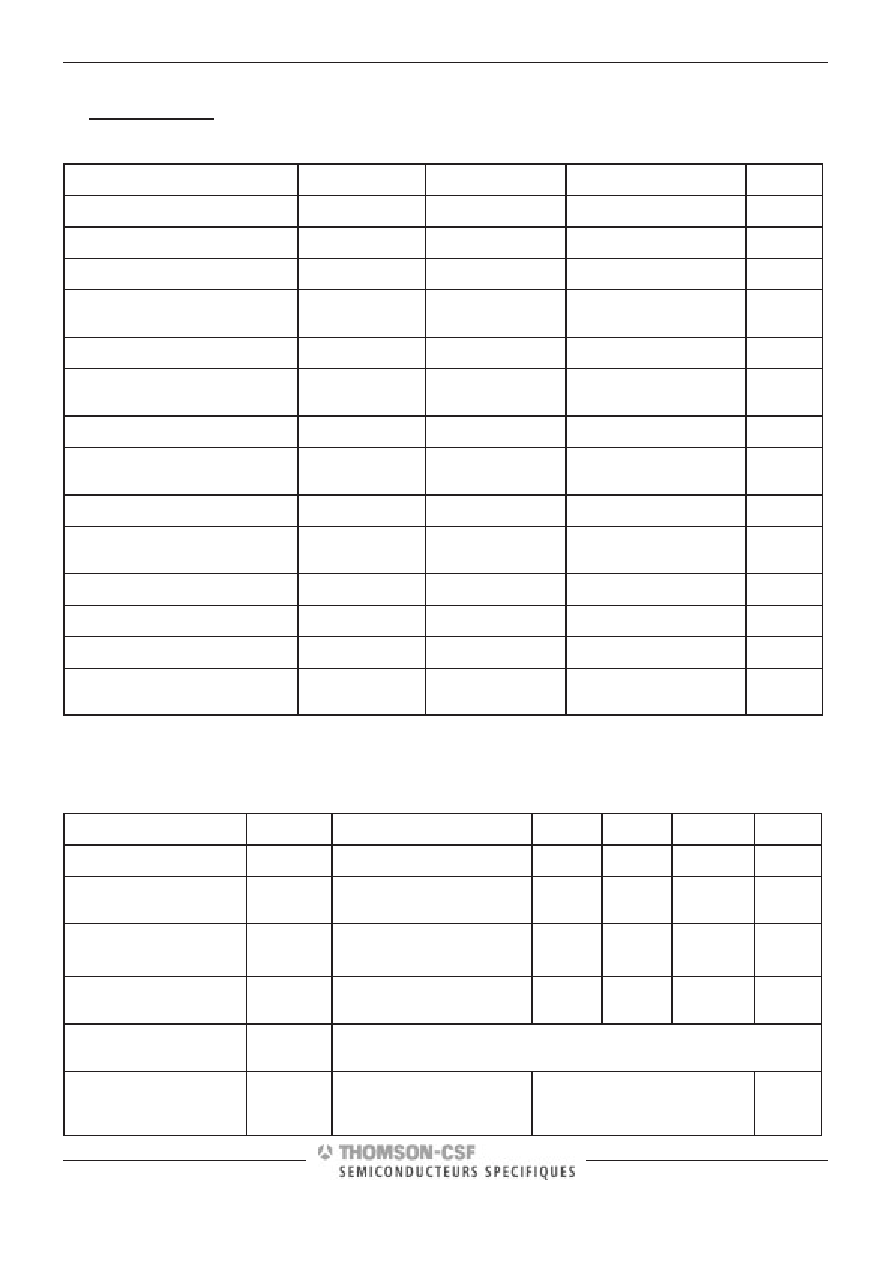
3. SPECIFICATIONS
3.1.
ABSOLUTE MAXIMUM RATINGS
(see note below)
Parameter
Symbol
Comments
Value
Unit
Positive Supply Voltage
VCC
GND to 6
V
Digital Negative Supply voltage
DVEE
GND to –5.7
V
Negative supply voltage
VEE
GND to –6
V
Maximum
difference
between
negative supplies
DVEE to VEE
0.3
V
Analog input voltages
VIN or VINB
–1 to +1
V
Maximum difference between VIN
and VINB
VIN –VINB
–1 to +1
V
Digital input voltage
VD
GORB
–0.3 to VCC +0.3
V
Digital output current
IO
Conditions :
–3V<Vout < 0.5 V
20
mA
Clock input voltage
VCLK or VCLKB
–3 to +1.5
V
Maximum
difference
between
VCLK and VCLKB
VCLK – VCLKB
–2 to +2
V
Maximum junction temperature
Tj
+145
°C
Operating temperature (Tc)
Top
–55 to +125
°C
Storage temperature
Tstg
–65 to +150
°C
Lead temperature
(soldering 10 s)
Tleads
+300
°C
Notes : Absolute maximum ratings are limiting values, to be applied individually, while other parameters are within specified operat-
ing conditions. Long exposure to maximum rating may affect device reliability.
The use of a thermal heat sink is mandatory (see Thermal characteristics page 15).
3.2.
RECOMMENDED CONDITIONS OF USE
Parameter
Symbol
Comments
Min.
Typ.
Max.
Unit
Positive supply voltage
VCC
4.75
+5
5.25
V
Negative supplies volt-
ages
VEE, DVEE
–5.25
–5.0
–4.75
V
Differential analog input
voltage (Full Scale)
VIN, VINB
VIN –VINB
50 ohms differential or
single–ended
±125
500
mV
mVpp
Clock input power level
PCLK,
PCLKB
50
W single-ended clock
input
4
10
dBm
Digital Outputs termina-
tion
ZOUT
75
W or 50 W differential output back termination, or unterminated out-
puts : see Advanced Application Notes figures 3,4,5
Operating temperature
range
TJ
Civil : ”C” grade
Industrial : ”V” grade
Military : ”M” grade
0 < Tc < 70
–40 < Tc < 85
–55 < Tc ; Tj < +125
°C
相關PDF資料 |
PDF描述 |
|---|---|
| TS8387VF | 1-CH 8-BIT PROPRIETARY METHOD ADC, PARALLEL ACCESS, CQFP68 |
| TS8387MF | 1-CH 8-BIT PROPRIETARY METHOD ADC, PARALLEL ACCESS, CQFP68 |
| TS8387VF_ | 1-CH 8-BIT PROPRIETARY METHOD ADC, PARALLEL ACCESS, CQFP68 |
| TS12A4516P | 1-CHANNEL, SGL POLE SGL THROW SWITCH, PDIP8 |
| TS2007EIJT | 3 W, 1 CHANNEL, AUDIO AMPLIFIER, PBGA9 |
相關代理商/技術參數 |
參數描述 |
|---|---|
| TS8388B | 制造商:ATMEL 制造商全稱:ATMEL Corporation 功能描述:ADC 8-bit 1 GSPS |
| TS8388BCF | 制造商:e2v technologies 功能描述:ADC 8-BIT 1 GSPS - Trays |
| TS8388BCFS | 制造商:e2v technologies 功能描述:ADC 8-BIT 1 GSPS - Trays |
| TS8388BCG | 制造商:未知廠家 制造商全稱:未知廠家 功能描述:A/D CONVERTER |
| TS8388BCGL | 制造商:e2v technologies 功能描述:ADC 8-BIT 1 GSPS - Trays |
發布緊急采購,3分鐘左右您將得到回復。