- 您現在的位置:買賣IC網 > PDF目錄98299 > TS8388BMFS9NB2 (E2V TECHNOLOGIES PLC) 1-CH 8-BIT PROPRIETARY METHOD ADC, PARALLEL ACCESS, CQFP68 PDF資料下載
參數資料
| 型號: | TS8388BMFS9NB2 |
| 廠商: | E2V TECHNOLOGIES PLC |
| 元件分類: | ADC |
| 英文描述: | 1-CH 8-BIT PROPRIETARY METHOD ADC, PARALLEL ACCESS, CQFP68 |
| 封裝: | CERAMIC, QFP-68 |
| 文件頁數: | 25/62頁 |
| 文件大小: | 1267K |
| 代理商: | TS8388BMFS9NB2 |
第1頁第2頁第3頁第4頁第5頁第6頁第7頁第8頁第9頁第10頁第11頁第12頁第13頁第14頁第15頁第16頁第17頁第18頁第19頁第20頁第21頁第22頁第23頁第24頁當前第25頁第26頁第27頁第28頁第29頁第30頁第31頁第32頁第33頁第34頁第35頁第36頁第37頁第38頁第39頁第40頁第41頁第42頁第43頁第44頁第45頁第46頁第47頁第48頁第49頁第50頁第51頁第52頁第53頁第54頁第55頁第56頁第57頁第58頁第59頁第60頁第61頁第62頁
31
0860E–BDC–05/07
e2v semiconductors SAS 2007
TS8388B
8.3.2
Differential vs. Single-ended Analog Input Operation
The TS8388B can operate at full speed in either differential or single-ended configuration.
This is explained by the fact the ADC uses a high input impedance differential preamplifier stage, (pre-
ceeding the sample and hold stage), which has been designed in order to be entered either in differential
mode or single-ended mode.
This is true so long as the out-of-phase analog input pin V
INB is 50 terminated very closely to one of the
neighboring shield ground pins (52, 53, 58, 59) which constitute the local ground reference for the
inphase analog input pin (V
IN).
Thus the differential analog input preamplifier will fully reject the local ground noise (and any capacitively
and inductively coupled noise) as common mode effects.
In typical single-ended configuration, enter on the (V
IN) input pin, with the inverted phase input pin (VINB)
grounded through the 50
termination resistor.
In single-ended input configuration, the in-phase input amplitude is 0.5V peak to peak, centered on 0V
(or -2 dBm into 50
). The inverted phase input is at ground potential through a 50 termination resistor.
However, dynamic performances can be somewhat improved by entering either analog or clock inputs in
differential mode.
8.3.3
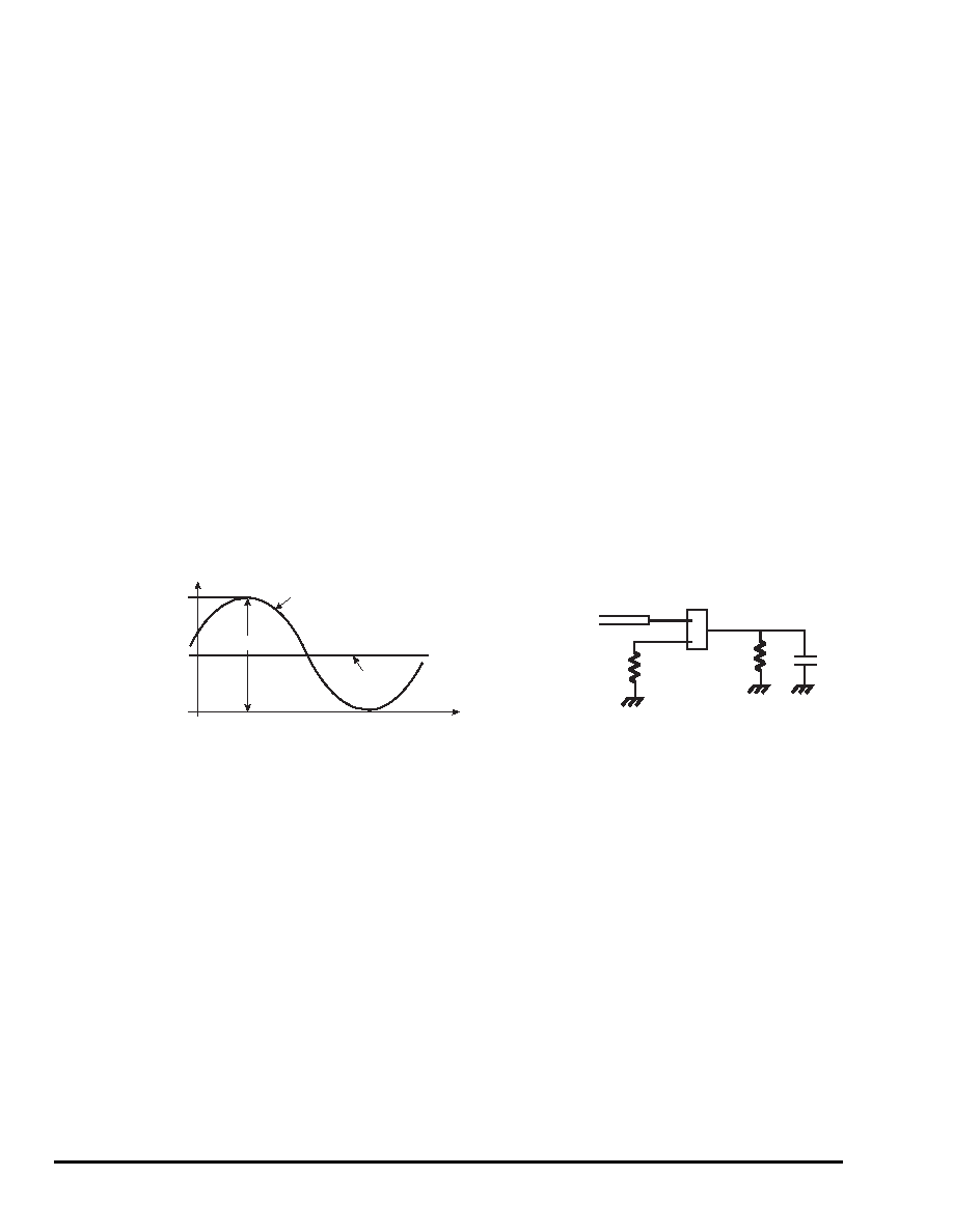
Typical Single-ended Analog Input Configuration
Figure 8-2.
Typical Single-ended Analog Input Configuration
Note:
Since VIN and VINB have a double pad architecture, a 50
reverse termination is needed. For the CBGA
package, this reverse termination is already on package.
8.4
Clock Inputs (CLK) (CLKB)
The TS8388B can be clocked at full speed without noticeable performance degradation in either differen-
tial or single-ended configuration.
This is explained by the fact the ADC uses a differential preamplifier stage for the clock buffer, which has
been designed in order to be entered either in differential or single-ended mode.
Recommended sinewave generator characteristics are typically –120 dBc/Hz phase noise floor spectral
density, at 1 kHz from carrier, assuming a single tone 4 dBm input for the clock signal.
8.4.1
Single-ended Clock Input (Ground Common Mode)
Although the clock inputs were intended to be driven differentially with nominal –0.8V/–1.8V ECL levels,
the TS8388B clock buffer can manage a single-ended sinewave clock signal centered around 0V. This is
the most convenient clock input configuration as it does not require the use of a power splitter.
50
(external or
on package)
1 M
3 pF
-250
250
500 mV
t
[mV]
VIN
VIN =
±250 mV = 500 mV diff
VIN or VINB double pad (pins 54, 55 or 56, 57)
VIN or VINB
50
reverse termination
500 mV
Full Scale
analog input
VINB = 0V
VINB
相關PDF資料 |
PDF描述 |
|---|---|
| TS8388BMFS9NB3 | 1-CH 8-BIT PROPRIETARY METHOD ADC, PARALLEL ACCESS, CQFP68 |
| TS8388BMFS9NC2 | 1-CH 8-BIT PROPRIETARY METHOD ADC, PARALLEL ACCESS, CQFP68 |
| TS8388BMFSB/Q | 1-CH 8-BIT PROPRIETARY METHOD ADC, PARALLEL ACCESS, CQFP68 |
| TS8388BVF | 1-CH 8-BIT PROPRIETARY METHOD ADC, PARALLEL ACCESS, CQFP68 |
| TS8388BMFS9NC3 | 1-CH 8-BIT PROPRIETARY METHOD ADC, PARALLEL ACCESS, CQFP68 |
相關代理商/技術參數 |
參數描述 |
|---|---|
| TS8388BMFS9NB3 | 制造商:ATMEL 制造商全稱:ATMEL Corporation 功能描述:ADC 8-bit 1 GSPS |
| TS8388BMFS9NC2 | 制造商:ATMEL 制造商全稱:ATMEL Corporation 功能描述:ADC 8-bit 1 GSPS |
| TS8388BMFS9NC3 | 制造商:ATMEL 制造商全稱:ATMEL Corporation 功能描述:ADC 8-bit 1 GSPS |
| TS8388BMFSB/Q | 制造商:e2v technologies 功能描述:ADC 8-BIT 1 GSPS - Trays |
| TS8388BVF | 制造商:e2v technologies 功能描述:ADC 8-BIT 1 GSPS - Trays |
發布緊急采購,3分鐘左右您將得到回復。